

Static random access memory (SRAM) device
- Summary
- Abstract
- Description
- Claims
- Application Information
AI Technical Summary
Benefits of technology
Problems solved by technology
Method used
Image

Examples
first embodiment
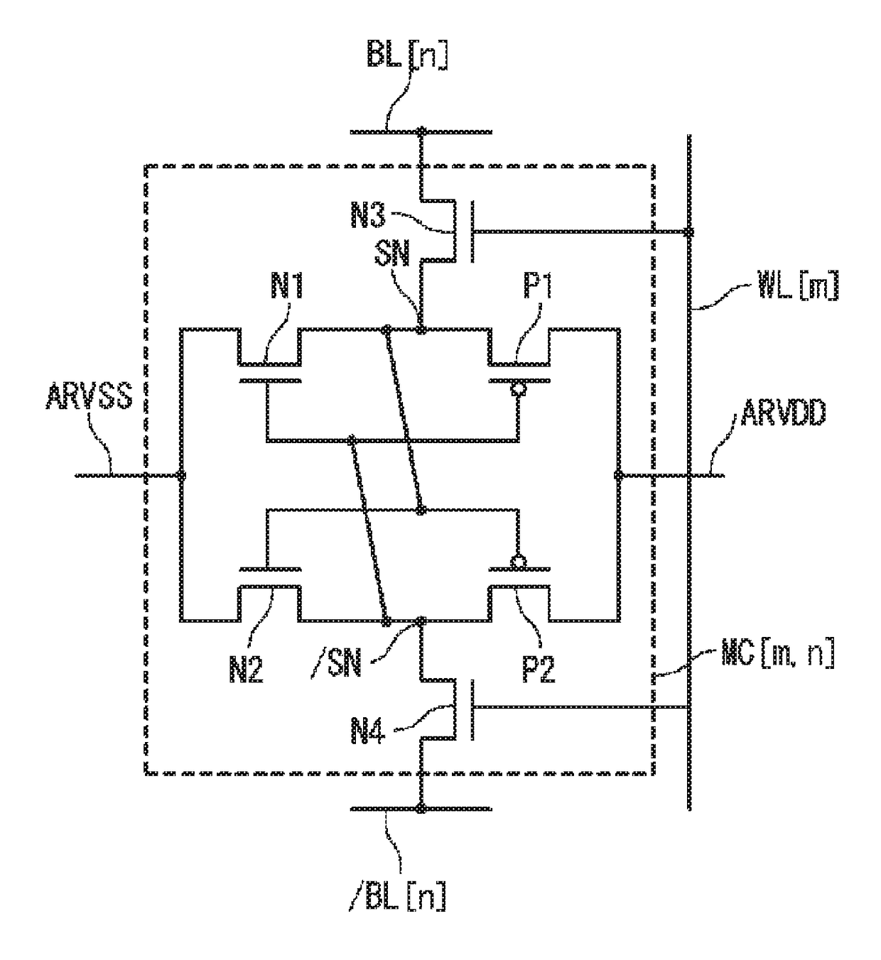
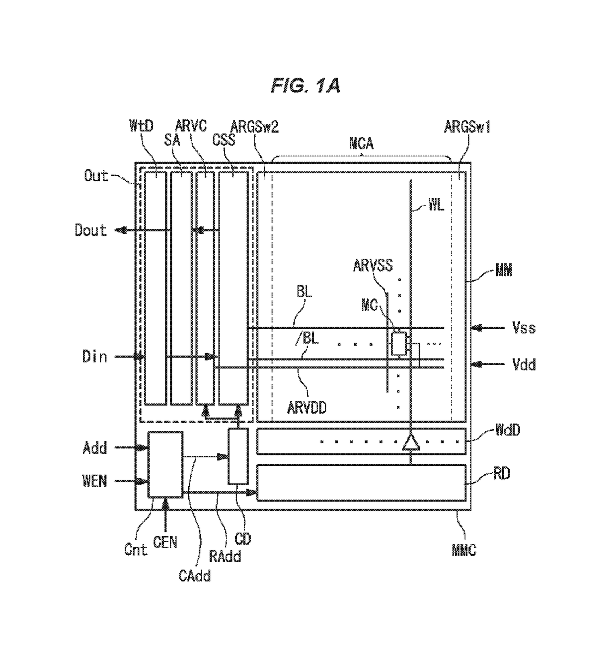
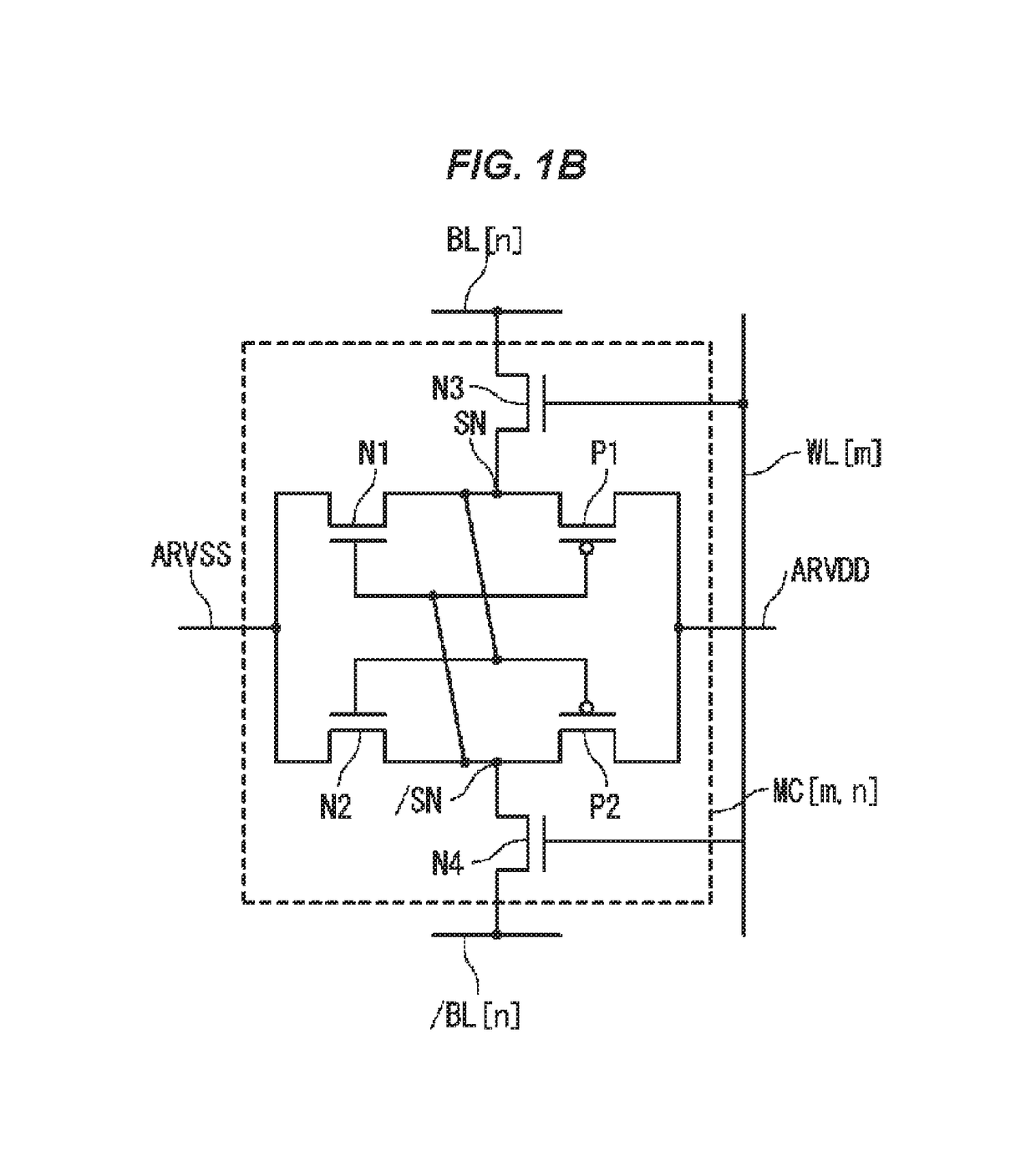
[0040]FIG. 1A is a plan block circuit diagram schematically showing the overall configuration of a typical SRAM. The configuration of the SRAM shown in FIG. 1A is described. This SRAM includes a memory mat circuit MM, an output circuit Out, a word driver circuit WdD, a row decoder RD, a control circuit Cnt, a column decoder CD, a word line WL, a first bit line BL and a second bit line / BL constituting a bit line pair, a cell power supply line ARVDD, and a local ground line ARVSS. Here, the bit line pair BL and / BL, the cell power supply line ARVDD, and the local ground line ARVSS are preferably provided in plural numbers, respectively.
[0041]The memory mat circuit MM includes a memory cell array MCA, a first ground line switch circuit ARGSw1, and a second ground line switch circuit ARGSw2. The memory cell array MCA includes a plurality of memory cells MC arranged in a vertical and horizontal array.
[0042]The output circuit Out includes a column selection switch circuit CSS, a cell pow...
second embodiment
[0137]FIG. 3A is a plan view showing the configuration of a wiring portion 3 according to a second embodiment. The components of the wiring portion 3 shown in FIG. 3A are described. The wiring portion 3 shown in FIG. 3A includes the external power supply voltage lines VDD3 and VDD51 to VDD54, the external ground voltage lines VSS3 and VSS51 to VSS54, the local ground line ARVSS3, and the vias V.
[0138]Here, the external power supply voltage lines VDD51 to VDD54 and the external ground voltage lines VSS51 to VSS54 shown in FIG. 3A are assumed to be identical to the external power supply voltage lines VDD51 to VDD54 and the external ground voltage lines VSS51 to VSS54 shown in FIG. 1G, respectively. Moreover, the external power supply voltage line VDD3, the external ground voltage line VSS3, and the local ground line ARVSS3 shown in FIG. 3A are assumed to correspond to the external power supply voltage line VDD42, the external ground voltage line VSS42, and the local ground line ARVSS4...
third embodiment
[0145]FIG. 4A is a plan view showing the configuration of a wiring portion 4 according to a third embodiment. The components of the wiring portion 4 shown in FIG. 4A are described. The wiring portion 4 shown in FIG. 4A includes the external power supply voltage lines VDD4 and VDD51 to VDD54, the external ground voltage lines VSS4 and VSS51 to VSS54, the local ground line ARVSS4, and the vias V.
[0146]Here, the external power supply voltage lines VDD51 to VDD54 and the external ground voltage lines VSS51 to VSS54 shown in FIG. 4A are assumed to be identical to the external power supply voltage lines VDD51 to VDD54 and the external ground voltage lines VSS51 to VSS54 shown in FIG. 1G, respectively. However, in FIG. 4A, the arrangement is exchanged between the external power supply voltage line VDD51 and the external ground voltage line VSS51.
[0147]Moreover, the external power supply voltage line VDD4, the external ground voltage line VSS4, and the local ground line ARVSS4 shown in FIG....
PUM
 Abstract
Description
Claims
Application Information