Skew adjustment circuit, semiconductor device, and skew calibration method

a technology of skew and adjustment circuit, which is applied in the direction of pulse manipulation, pulse technique, baseband system details, etc., can solve the problems of difficult sampling of input signals, erroneous operation, and difficulty in reducing the variation of phase intervals between clock signals, so as to reduce erroneous operation

Inactive Publication Date: 2017-08-01
HITACHI LTD
View PDF11 Cites 5 Cited by
  • Summary
  • Abstract
  • Description
  • Claims
  • Application Information

AI Technical Summary

Benefits of technology

[0010]Due to the fact that the transfer rate is increased, a period of the data to be transmitted is shortened. Therefore, it is also required to shorten a period of the clock signal for sampling the input signal. When variation is generated in phase intervals between the clock signals for sampling due to variation during manufacturing of a semiconductor device having the CDR circuit and environmental change such as temperature change of when the semiconductor device is used, it becomes difficult to sample the input signal at an appropriate timing, and it leads to erroneous operation. Therefore, it is required to prevent that variation is generated in the phase intervals between the clock signals for sampling.
[0015]In an embodiment, a skew adjustment circuit includes: a plurality of latch circuits for taking in an input signal in response to the plurality of first clock signals; a phase adjustment circuit for adjusting phases of a plurality of second clock signals, based on the plurality of second clock signals generated based on a reference clock signal and output signals from the plurality of latch circuits; a phase interval detection circuit for detecting phase intervals between the plurality of first clock signals, based on a reference value; and a phase interval adjustment circuit for performing adjustment such that phase intervals become equal to each other between the plurality of second clock signals adjusted by the phase adjustment circuit, based on a skew adjustment signal from the phase interval detection circuit. Here, the reference value is obtained by calibration, and the plurality of second clock signals adjusted by the phase interval adjustment circuit is provided as the plurality of first clock signals to the plurality of latch circuits. The phase intervals are determined to be equal to each other between the plurality of first clock signals for determining timing when each of the latch circuits takes in the input signal, based on the reference value obtained by the calibration. Thus, it becomes possible to suppress that timing when each of the latch circuits takes in the input signal varies, and reduction of erroneous operation can be achieved.
[0017]Further, in an embodiment, a skew calibration method is provided for correcting a skew between a plurality of clock signals having different phases from each other. The provided skew calibration method includes: a phase interval detection process for obtaining a time difference (phase interval) between the clock signals being close to each other, in the plurality of clock signals formed based on a reference clock signal; and an operation process for obtaining a total of the time difference obtained in the phase interval detection process for the plurality of clock signals and for obtaining the reference value by dividing the obtained total by the number of the plurality of clock signals, and phases of the clock signals are adjusted (corrected) by the reference value obtained in the operation process. In the plurality of clock signals formed based on the reference clock signal, the total of the time difference between the clock signals being close to each other corresponds to one period of the reference clock signal. Therefore, even when the phase intervals vary between particular clock signals, total time does not vary. Therefore, the reference value that is not affected by variation can be obtained by dividing the total time by the number of the clock signals formed. Since the phases of the clock signals are corrected using the reference value that is not affected by the variation, reduction of erroneous operation can be achieved.

Problems solved by technology

When variation is generated in phase intervals between the clock signals for sampling due to variation during manufacturing of a semiconductor device having the CDR circuit and environmental change such as temperature change of when the semiconductor device is used, it becomes difficult to sample the input signal at an appropriate timing, and it leads to erroneous operation.
In JP-2008-66879-A, it is stated that reducing the variation of the phase intervals between the clock signals is difficult when the plurality of clock signals is formed using one reference clock signal.

Method used


Image

  • Skew adjustment circuit, semiconductor device, and skew calibration method
  • Skew adjustment circuit, semiconductor device, and skew calibration method
  • Skew adjustment circuit, semiconductor device, and skew calibration method

Examples


first embodiment

[0032]

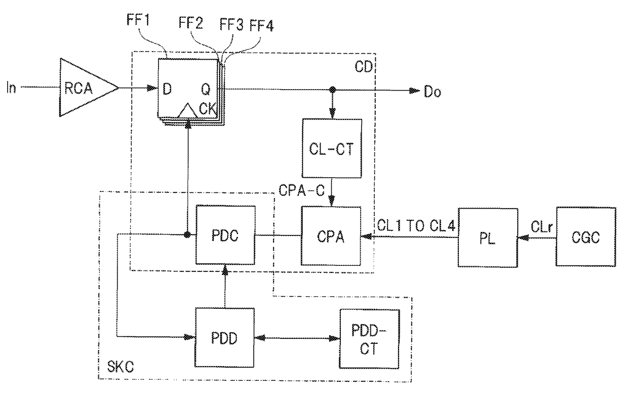
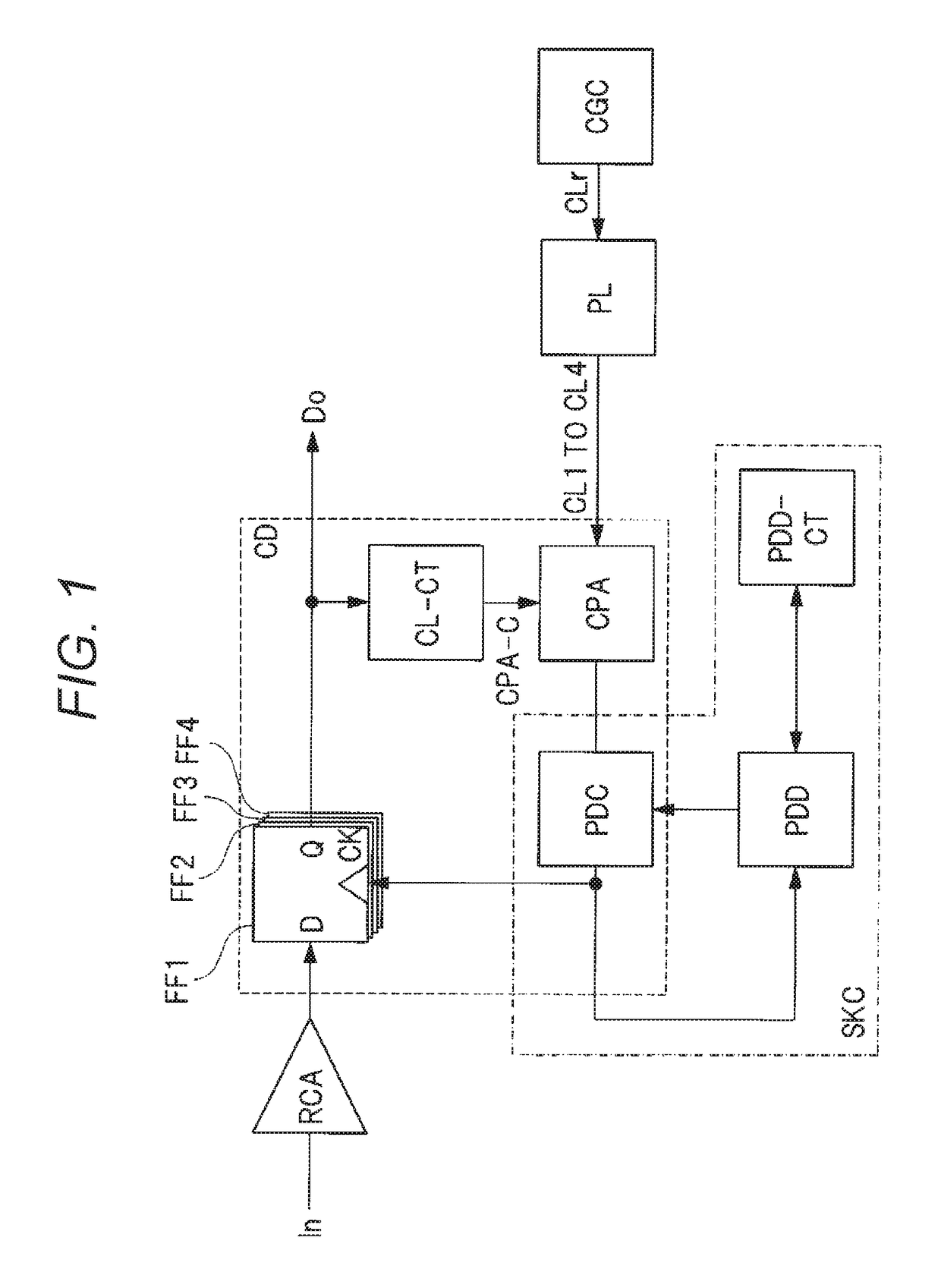
[0033]FIG. 8 is a schematic sectional view illustrating a configuration of an electronic apparatus using a semiconductor device according to a first embodiment. In FIG. 8, an information communication apparatus 100 is an electronic apparatus. The information communication apparatus 100, although it is not particularly limited, includes a back plane BP on which a plurality of connectors CNT1-CNTn is mounted, and cards RCD1-RCDn attached to the connectors CNT1-CNTn.

[0034]In the back plane BP, multiple wirings are formed for electrically connecting the connectors CNT1-CNTn to each other, and the wirings become transmission lines when data are transmitted between the connectors CNT1-CNTn. In FIG. 8, the transmission lines configured by the wirings formed on the back plane BP are illustrated as DLL(1)-DLL(i). In addition, for convenience of description, the transmission line used for data transmission between the connector CNT1 and the connector CNTn is illustrated as the DLL(1), a...

second embodiment

[0161]FIG. 7 is a flowchart diagram illustrating operation of the skew adjustment circuit SKC according to a second embodiment. In the first embodiment, as described in FIG. 4, the operation has been performed in which the reference value of the phase interval is obtained in the calibration period, and the phase interval is adjusted between the clock signals being close to each other by using the reference value obtained. That is, in the example illustrated in FIG. 4, first, adjustment operation is performed so that the phase interval between the clock signals CL1-AA and CL2-AA being close to each other is matched with the reference value, and the phase interval between the clock signals CL1-AA and CL2-AA is adjusted to be matched with the reference value, and then the phase interval between the clock signals CL2-AA whose phase is adjusted to the clock signal CL1-AA and the clock signal CL3-AA is adjusted to be matched with the reference value. In addition, after the phase interval ...


PUM


Abstract

A skew adjustment circuit includes: flip flop circuits for taking in an input signal in response to first clock signals; a clock phase adjustment circuit for adjusting phases of second clock signals, based on the second clock signals generated based on a reference clock signal and an output signal from the flip flop circuits; a phase interval detection circuit for detecting a phase interval between the first clock signals, based on a reference value; and a phase interval adjustment circuit for performing adjustment such that phase intervals become equal to each other between the second clock signals adjusted by the clock phase adjustment circuit, based on a skew adjustment signal from the phase interval detection circuit. The reference value is obtained by calibration, and the second clock signals adjusted by the phase interval adjustment circuit are provided as the first clock signals to the flip flop circuits.

Description

BACKGROUND OF THE INVENTION[0001]1. Field of the Invention[0002]The present invention relates to a skew adjustment circuit, a semiconductor device, and a skew calibration method, and in particular relates to the skew adjustment circuit of a clock signal used in a Clock and Data Recovery circuit (hereinafter referred to as a CDR circuit), and the semiconductor device including the CDR circuit.[0003]2. Description of the Related Art[0004]Along with speeding up of information communication apparatuses, a transfer rate of data (data rate) has been increased for transferring the data between semiconductor devices configuring the information communication apparatuses. For example, it is expected that the transfer rate per channel to transfer the data reaches 25 Gbps in 2016 and the transfer rate is further increased. The semiconductor devices are mounted on a circuit board such as a printed circuit board, and transmission and reception of the data are performed via wiring of the circuit b...

Claims


Application Information

Patent Timeline
Patent Type & Authority Patents(United States)
IPC IPC(8): H04L7/00H03K5/15H03L7/08H04L7/033
CPCH03K5/15066H03L7/0807H04L7/033H03L7/0814H04L25/14
Inventor USUGI, TATSUNORIKURITA, KOUZABUROUKOMORI, TAKEMASANASU, JUNYA
Owner HITACHI LTD
Why Eureka
Try Eureka