
Micromechanical sensor device and corresponding manufacturing method

a sensor device and micromechanical technology, applied in the direction of fluid speed measurement, instruments, coatings, etc., can solve the problems of affecting the reliability of the bond, and the possibility of providing the contact area, so as to improve the bond reliability

Active Publication Date: 2017-08-08
ROBERT BOSCH GMBH
View PDF6 Cites 2 Cited by
  • Summary
  • Abstract
  • Description
  • Claims
  • Application Information

AI Technical Summary

Benefits of technology

The present invention provides a micromechanical sensor device that includes a MEMS substrate and an ASIC substrate with a reliable mechanical or electrical connection between them. This connection reduces sensitivity to stress and allows for smaller contact areas. The device is compatible with commonly used manufacturing processes and can also be combined with other measures to further reduce sensitivity. The one-sided elastic suspension prevents overloading of the contact area, and a signal entry into the ASIC chip is facilitated by the electrical contact element with a perforation. The spring element is under pretensioning, improving bond reliability for small contact areas. These technical effects improve the performance, reliability, and sensitivity of the micromechanical sensor device.

Problems solved by technology

One of the great challenges of chip scale packages for MEMS sensor devices is the control of stress effects.
Since a very large number of contacts are required, it is not possible to provide these contacts with a very large, and thus mechanically stable, design.
However, in the separation process, usually a sawing process, contact areas 52 are very close to the cutting line, and experience vibrations which may emanate from that location and damage contact areas 52.
In the middle of the chip, contact areas 52 experience high mechanical stress during the bonding process, and may be damaged.
The MEMS substrate is therefore very sensitive to external stress, which reduces the service life.

Method used


Image

  • Micromechanical sensor device and corresponding manufacturing method
  • Micromechanical sensor device and corresponding manufacturing method
  • Micromechanical sensor device and corresponding manufacturing method

Examples


Embodiment Construction

[0039]Identical or functionally equivalent elements are denoted by the same reference numerals in the figures.

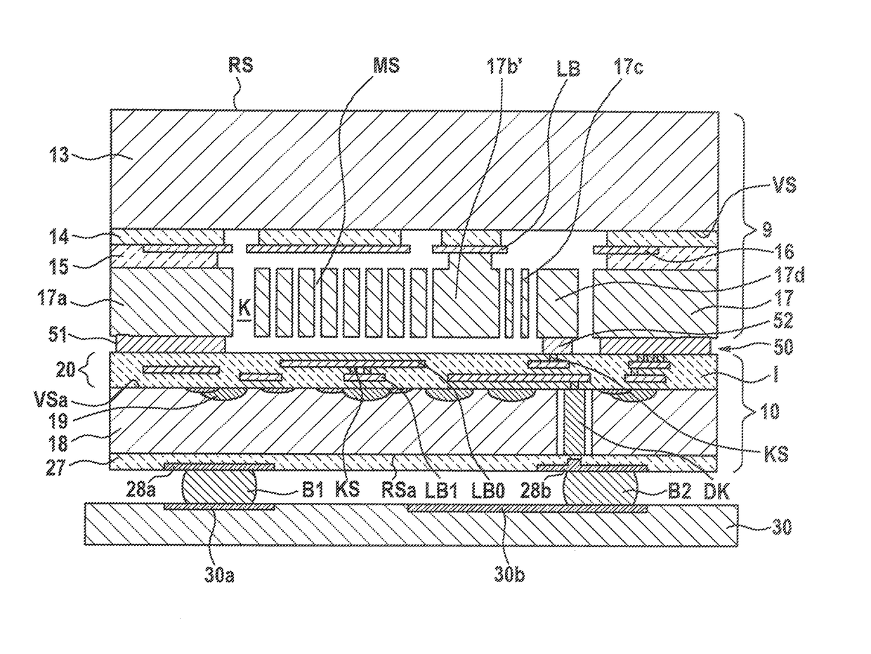
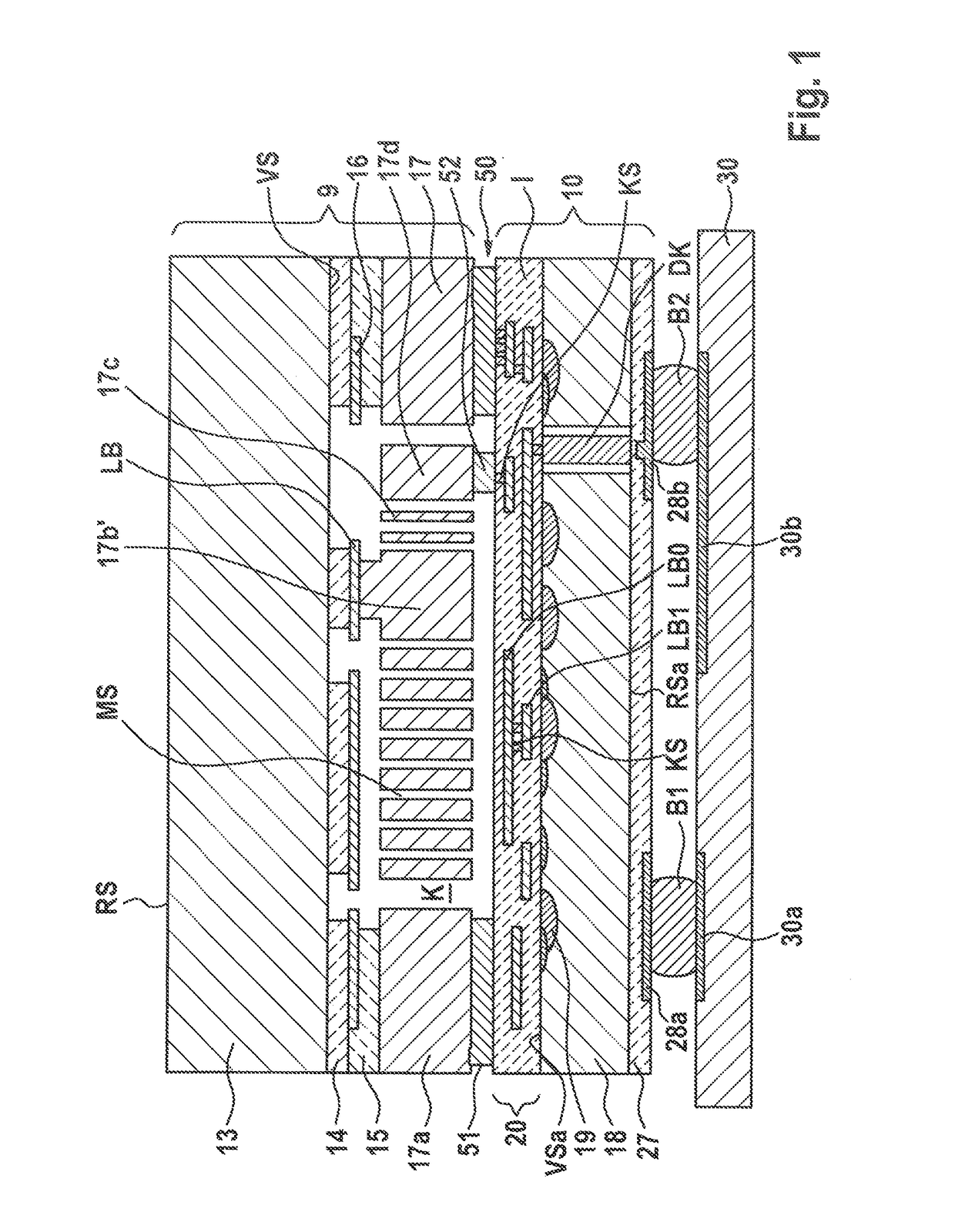
[0040]FIG. 1 shows a schematic cross-sectional view for explaining a micromechanical sensor device according to a first specific embodiment of the present invention.

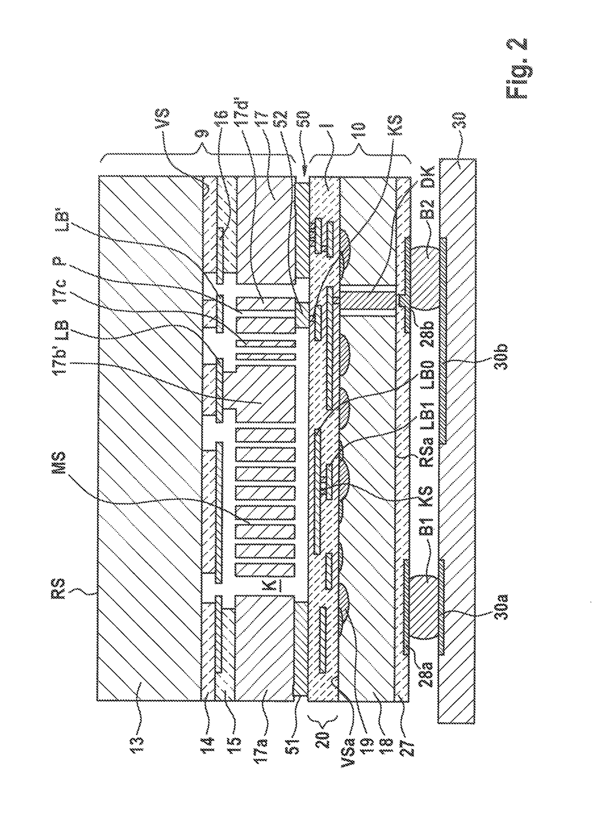
[0041]The first specific embodiment of the micromechanical sensor device according to the present invention illustrated in FIG. 1 differs from the example of the sensor device according to FIG. 4 in the configuration and coupling of second micromechanical functional layer 17.

[0042]According to FIG. 1, micromechanical functional layer 17, the same as that according to FIG. 4, includes a rigid anchoring area 17a at the edge which is connected to movable sensor structure MS. Also provided is a first anchoring area 17b′ which is formed in second micromechanical functional layer 17 and which on one side is anchored on a conductor area LB on first micromechanical functional layer 16 of MEMS substrate 9.

[0043]An electri...


PUM

PropertyMeasurementUnit
temperaturesaaaaaaaaaa
anchoring areaaaaaaaaaaa
areaaaaaaaaaaa

Abstract

A micromechanical sensor device includes: an ASIC substrate having a first front side and a first rear side; a rewiring element formed on the first front side and including multiple stacked conductor levels and insulating layers; a MEMS substrate having a second front side and a second rear side; a first micromechanical functional layer formed on top of the second front side; and a second micromechanical functional layer formed on top of the first micromechanical functional layer and connected to the rewiring element. In the second micromechanical functional layer, a movable sensor structure is anchored on one side via a first anchoring area, and an electrical connecting element formed in a second anchoring area is anchored on one side on the ASIC, and the first and second anchoring areas are elastically connected to one another via a spring element.

Description

BACKGROUND OF THE INVENTION[0001]1. Field of the Invention[0002]The present invention relates to a micromechanical sensor device and a corresponding manufacturing method.[0003]2. Description of the Related Art[0004]Although any micromechanical components are applicable, the present invention and its underlying object to be achieved are explained with reference to components which include inertial sensors based on silicon.[0005]Micromechanical sensor devices for measuring acceleration, rotation rate, magnetic field, and pressure, for example, are generally known, and are mass-produced for various applications in the automotive and consumer sectors. In particular the miniaturization of components, functional integration, and effective cost reduction are trends in consumer electronics.[0006]Nowadays, acceleration sensors and rotation rate sensors, as well as acceleration sensors and magnetic field sensors, are already manufactured as combination sensors (6d), and in addition there are ...

Claims


Application Information

Patent Timeline
Patent Type & Authority Patents(United States)
IPC IPC(8): B81B7/00B81C1/00
CPCB81C1/00238B81B2207/07B81C2203/0792
Inventor GONSKA, JULIANREINMUTH, JOCHEN
Owner ROBERT BOSCH GMBH
Learn More