
Silicon nitride process for reduction of threshold shift

Active Publication Date: 2017-08-22
TEXAS INSTR INC
View PDF7 Cites 3 Cited by
  • Summary
  • Abstract
  • Description
  • Claims
  • Application Information

AI Technical Summary

Benefits of technology

The patent text describes a semiconductor device with a FET that has a layer of nitrogen-rich silicon nitride over its semiconductor region and under the gate. This layer helps to improve the device's performance and stability. The technical effect of this invention is to provide better performance and reliability for semiconductor devices.

Problems solved by technology

Charges tend to accumulate between the gate and the channel, in the gate dielectric layer, and thus adversely affect the reliability by shifting the threshold potential.
Charge accumulation is particularly problematic in gate dielectric layers which include silicon nitride.

Method used


Image

  • Silicon nitride process for reduction of threshold shift
  • Silicon nitride process for reduction of threshold shift
  • Silicon nitride process for reduction of threshold shift

Examples


Embodiment Construction

[0009]The present disclosure is described with reference to the attached figures. The figures are not drawn to scale and they are provided merely to illustrate the disclosure. Several aspects of the disclosure are described below with reference to example applications for illustration. It should be understood that numerous specific details, relationships, and methods are set forth to provide an understanding of the disclosure. One skilled in the relevant art, however, will readily recognize that the disclosure can be practiced without one or more of the specific details or with other methods. In other instances, well-known structures or operations are not shown in detail to avoid obscuring the disclosure. The present disclosure is not limited by the illustrated ordering of acts or events, as some acts may occur in different orders and / or concurrently with other acts or events. Furthermore, not all illustrated acts or events are required to implement a methodology in accordance with ...


PUM


Abstract

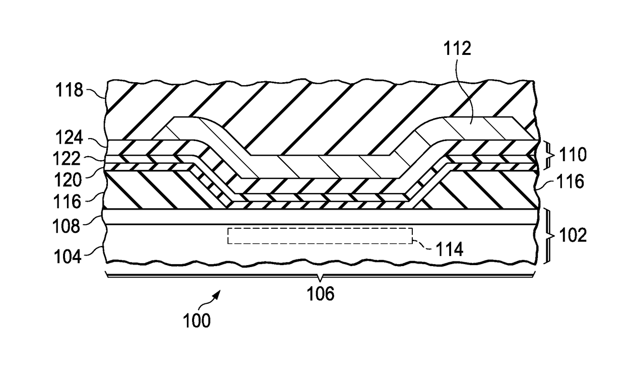
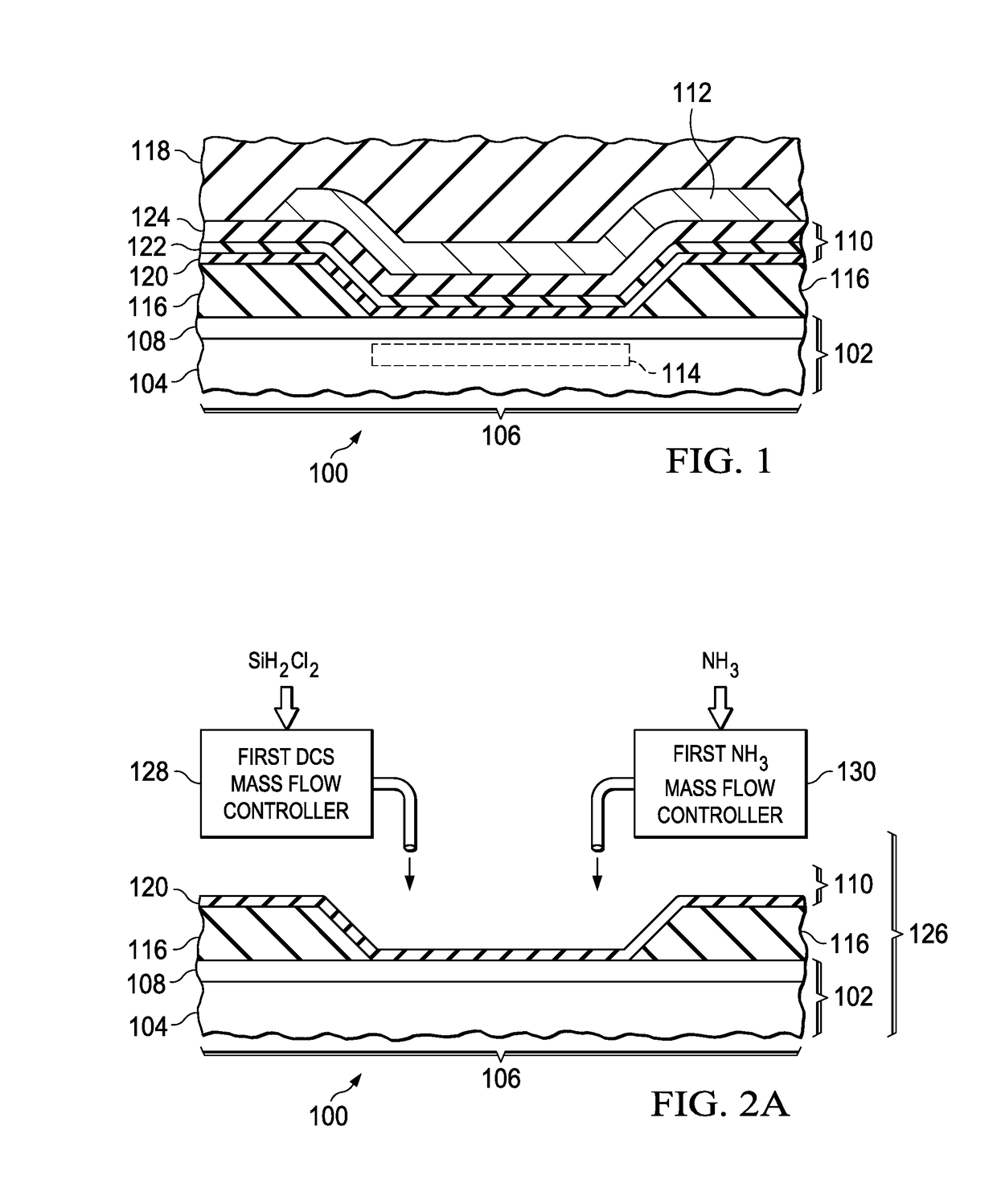
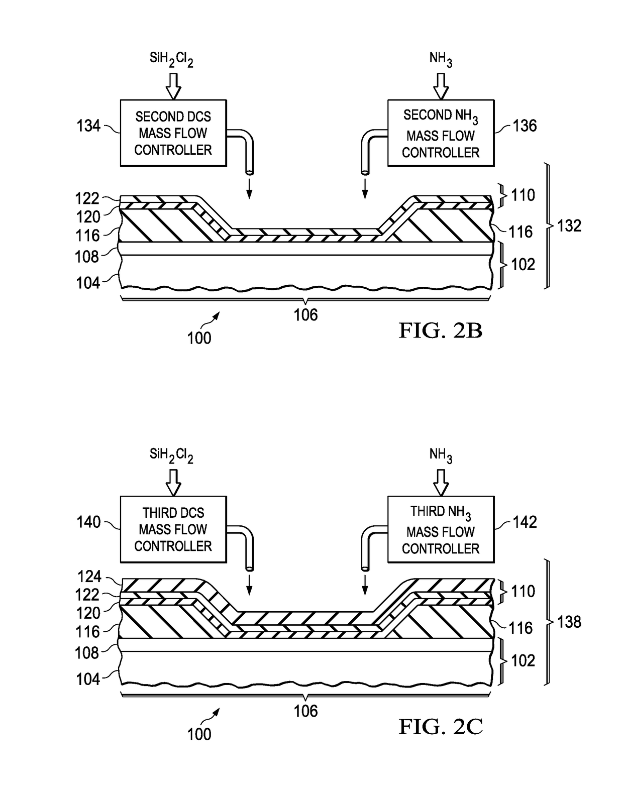
A semiconductor device has a substrate with a semiconductor material. The semiconductor device includes a field effect transistor in and on the semiconductor material. The field effect transistor has a gate dielectric layer over the semiconductor material of the semiconductor device, and a gate over the gate dielectric layer. The gate dielectric layer includes a layer of nitrogen-rich silicon nitride immediately over the region for the channel, and under the gate.

Description

FIELD[0001]This disclosure relates to the field of semiconductor devices. More particularly, this disclosure relates to field effect transistors in semiconductor devices.BACKGROUND[0002]A field effect transistor (FET) operates by applying a potential to the gate of the transistor, which changes the density of charge carriers in the channel of the transistor. The threshold potential of the transistor may be understood as the gate potential at which the transistor changes from the off state, in which minimal current flows through the channel, to the on state, in which a pre-defined current flows through the channel. Reliable operation of the transistor depends on the threshold potential remaining constant during the operational lifetime of the transistor. Charges tend to accumulate between the gate and the channel, in the gate dielectric layer, and thus adversely affect the reliability by shifting the threshold potential. Charge accumulation is particularly problematic in gate dielect...

Claims


Application Information

Patent Timeline
IPC IPC(8): H01L29/02H01L29/786H01L29/66H01L29/20H01L21/02
CPCH01L21/0228H01L29/2003H01L29/78606H01L29/66522H01L21/0254H01L21/0217H01L21/28264H01L29/513H01L29/518H01L29/7786H01L21/022H01L21/02211H01L21/02271
Inventor DELLAS, NICHOLAS STEPHENTIPIRNENI, NAVEENLEE, DONG SEUP
Owner TEXAS INSTR INC
Learn More