Organic light emitting diode and display panel using the same
a technology of light-emitting diodes and display panels, which is applied in the direction of basic electric elements, electrical apparatus, and semiconductor devices, can solve the problems of reducing the service life, reducing the injection efficiency, and reducing the light-emitting of devices, and achieves the effect of long service life and convenient preparation
- Summary
- Abstract
- Description
- Claims
- Application Information
AI Technical Summary
Benefits of technology
Problems solved by technology
Method used
Image

Examples
example 1
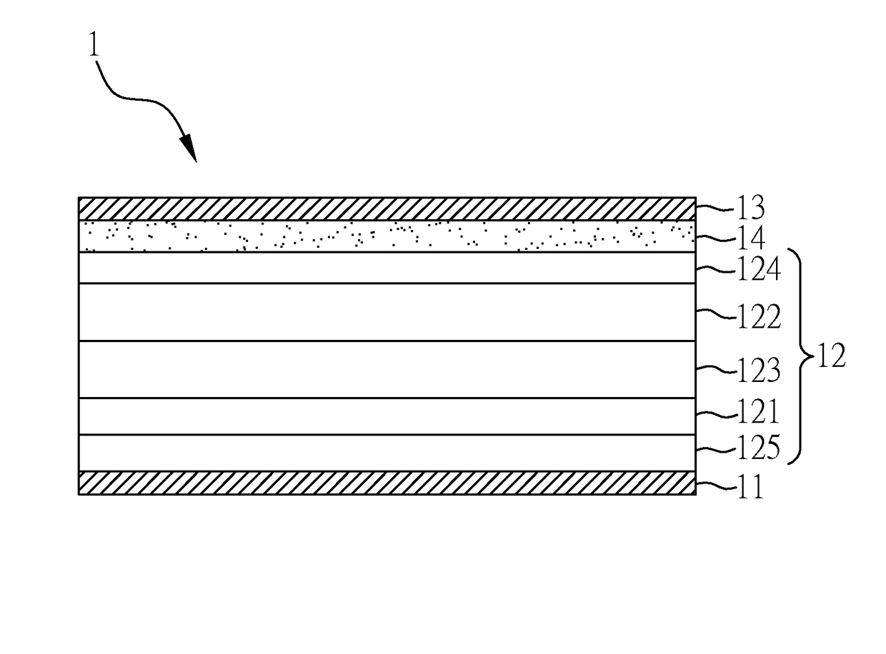
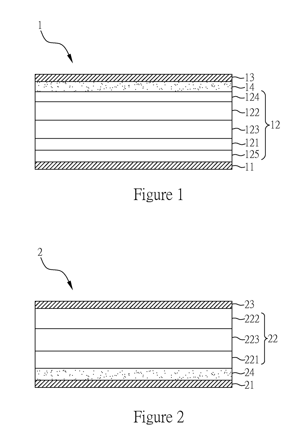
[0033]FIG. 1 shows a schematic structural view of an embodiment of the organic light emitting diode, comprising: a first electrode 11; an organic material layer 12, which includes a hole transport layer 121, an electron transport layer 122, and a light-light emitting layer 123, wherein the hole transport layer 121 is interposed between the first electrode 11 and the light-light emitting layer 123, the light emitting layer 123 is interposed between the hole transport layer 121 and the electron transport layer 122; a second electrode 13 provided on the organic material layer 12; a carrier conversion layer 14 interposed between the second electrode 13 and the electron transport layer 122; wherein the carrier conversion layer 14 is a P-doped carrier conversion layer having a thickness of 55 nm. In addition, to further improve the injection efficiency of electrons from the carrier conversion layer 14 to the electron transport layer 122, and injection efficiency of holes from the first el...
example 2
[0037]Example 2 was substantially similar to Example 1, except that the total thickness of the hole injection layer and the hole transport layer in Example 2 was 35 nm, while the carrier conversion layer had a thickness of 20 nm.
examples 3-5
[0038]Examples 3-5 were substantially similar to Example 2, except for the thickness of the carrier conversion layer, wherein the carrier conversion layer had a thickness of 60 nm in Example 3, 80 nm in Example 4, and 100 nm in Example 5. Accordingly, the organic light-emitting diodes having different carrier conversion layer thicknesses could be prepared.
PUM
 Abstract
Description
Claims
Application Information