Detection device for detecting photons and method therefore

a detection device and detection method technology, applied in measurement devices, instruments, radiation measurement, etc., can solve problems such as significant baseline estimates, significant time pickoff errors, and wrong registration of photon energy

Active Publication Date: 2017-09-12
KONINKLJIJKE PHILIPS NV
View PDF12 Cites 28 Cited by
  • Summary
  • Abstract
  • Description
  • Claims
  • Application Information

AI Technical Summary

Benefits of technology

[0023]In a further preferred embodiment of the invention, the compensation unit further comprises a baseline restorer circuit. By employing a baseline restorer circuit, a baseline shift can be mitigated. Further, baseline restoration reduces disadvantageous effects of low-frequency disturbances (e.g., power-line hum and vibrational microphonics).
[0024]In a further preferred embodiment of the invention, the detection device further comprises: a baseline restorer circuit, a switching network comprises first, second, third, and fourth switches, wherein the baseline restorer circuit is coupled between the first and second switches; and a current mirror. The detection device is operable in a first and a second mode. In the first mode, the first and second switches are closed so that the baseline restorer circuit is operable, the third switch couples a drain of the second transistor to the current mirror, and the fourth switch couples a drain of the first transistor to ground. In the second mode, the first and second switches are open, so that the baseline restorer circuit is disconnected and the third switch couples the drain of the second transistor to the drain of the first transistor. In the first mode, photoconductive gain is measured by measuring a compensation current via the current mirror. The second mode corresponds to normal operation.
[0025]In a further preferred embodiment of the invention, the detection device further comprises a fourth current source. The fourth current source is coupled between a drain of the second transistor and a drain of the first transistor. Preferably, the fourth current source is controlled by an output of the digital-to-analog converter so that the fourth current source may drain just the right amount of current so that the shaping element measures the photocurrent only.
[0026]In a further preferred embodiment of the invention, the detection device further comprises a digital-to-analog converter and an integrating channel, wherein the digital-to-analog converter is coupled between an output of the integrating channel and a control input of the fourth current source. The integrating channel may be used to determine the correct compensation current. The integrating channel's output may be provided to the digital-to-analog converter, which then, e.g., controls the fourth current source.
[0027]In a further preferred embodiment of the invention, the compensation unit comprises a baseline restorer circuit and a polarization determination unit. The polarization determination unit is adapted to determine a degree of polarization within the sensor from a baseline restorer current from the baseline restorer circuit. Thus, the idea of this preferred aspect is to detect or monitor the BLR feedback signal in order to use this to determine the grade of polarization within the sensor for every read-out impinging photon of the detector.
[0028]In a further preferred embodiment of the invention, the polarization determination unit further comprises an integrator circuit, wherein the integrator circuit is adapted to integrate a baseline restorer current from the baseline restorer circuit and to provide the baseline restorer current to the input of the shaping element. One reason for using an integrator is that the integrated signal is the mean or average of the BLR signal during the readout. For instance, the mean of the BLR signal during a readout period represents a good value to be monitored. Another candidate is the median of the BLR signal during a readout period.

Problems solved by technology

If Cd[Zn]Te with not fully blocking (cathode) contacts is used for single photon counting detectors, the photoconductive gain causes a major problem especially for DC coupled readout electronics: Since it is a slowly changing current on top of the photocurrent, it causes a baseline shift at the output of the analog readout channel towards the set energy thresholds so that, without any correction means, the energies of the photons is wrongly registered.
It is well-known that the conventional BLR approach of sensing the baseline (BL) at the output of the shaper (SHA) will result in significantly wrong baseline estimates, if pulses at the output of the SHA pile-up frequently: In this case, the BL is no longer reached so the BL is wrongly estimated.
Without pulse tail-cancellation, there are substantial errors in time pickoff due to the pulse pileup.

Method used


Image

  • Detection device for detecting photons and method therefore
  • Detection device for detecting photons and method therefore
  • Detection device for detecting photons and method therefore

Examples


first embodiment

[0060] which is described herein below, it is proposed to derive from the measured total pixel current and the determined photo-conductive gain (known from measurements), the compensation current, which is then provided by a current source.

[0061]Photoconductors with not fully blocking contacts exhibit a photoconductive gain PCG, i.e. the measured current when irradiated is much higher than the current, which results, if only the electron-hole pairs generated by impinging photons (optical or X-ray or other types) are considered, which current is called photocurrent Iphoto.

[0062]This also applies to direct conversion semiconductors like cadmium telluride (CdTe) and cadmium zinc telluride (CZT) currently investigated as conversion material for X-ray detectors to count individual X-ray photons for human computed tomography (CT) imaging. Note that any direct converting material with different transit times for holes and electrons will be polarized at a certain flux, as charge with the lo...

second embodiment

[0100] which is described herein below, it is proposed to detect or monitor the BLR feedback signal in order to use this to determine the grade of polarization within the sensor for every read-out impinging photon of the detector.

[0101]The effect of polarization in semiconductor x-ray sensor materials (e.g. CZT or CdTe) degrade the spectral performance of the detector as the collected charge at the pixelated cathode is decreased with increasing amount of polarization. FIG. 4(b) of Bale and Szeles, Nature of polarization in wide-bandgap semiconductor detectors under high-flux irradiation: Application to semi-insulating Cd1-xZnxTe, Phys. Rev. B 77, 035205 (2008), illustrates the resulting shift of the measured spectrum at four increasing flux rates (tube currents). The distortion of a detected pulse height spectrum as a function of the tube current is depicted. With increasing flux or tube current the spectrum gets shrunk.

[0102]Therefore the detected pulse height of an x-ray event ins...

third embodiment

[0110] which is described herein below, it is proposed to include a circuit at the input of the baseline restorer circuit that ensures that any signal above the baseline level is ignored.

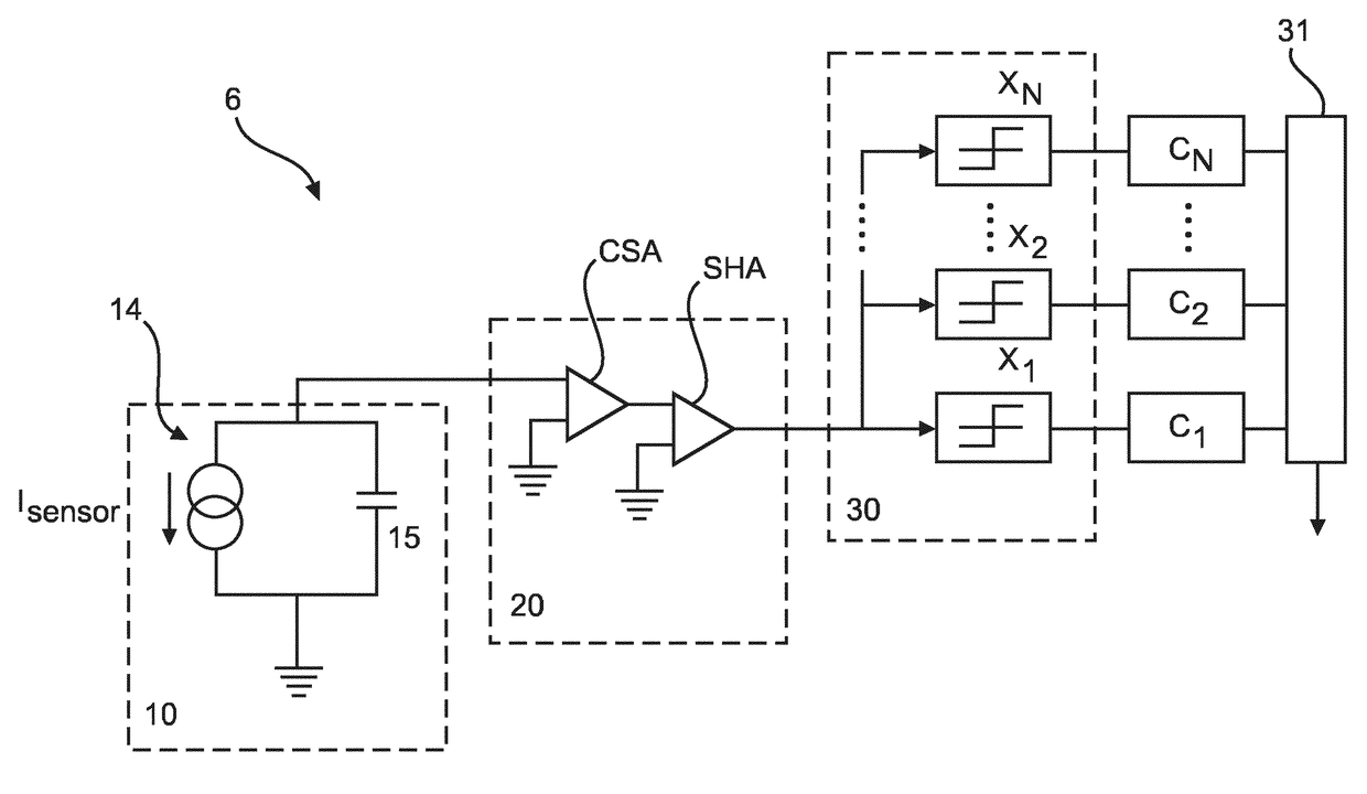
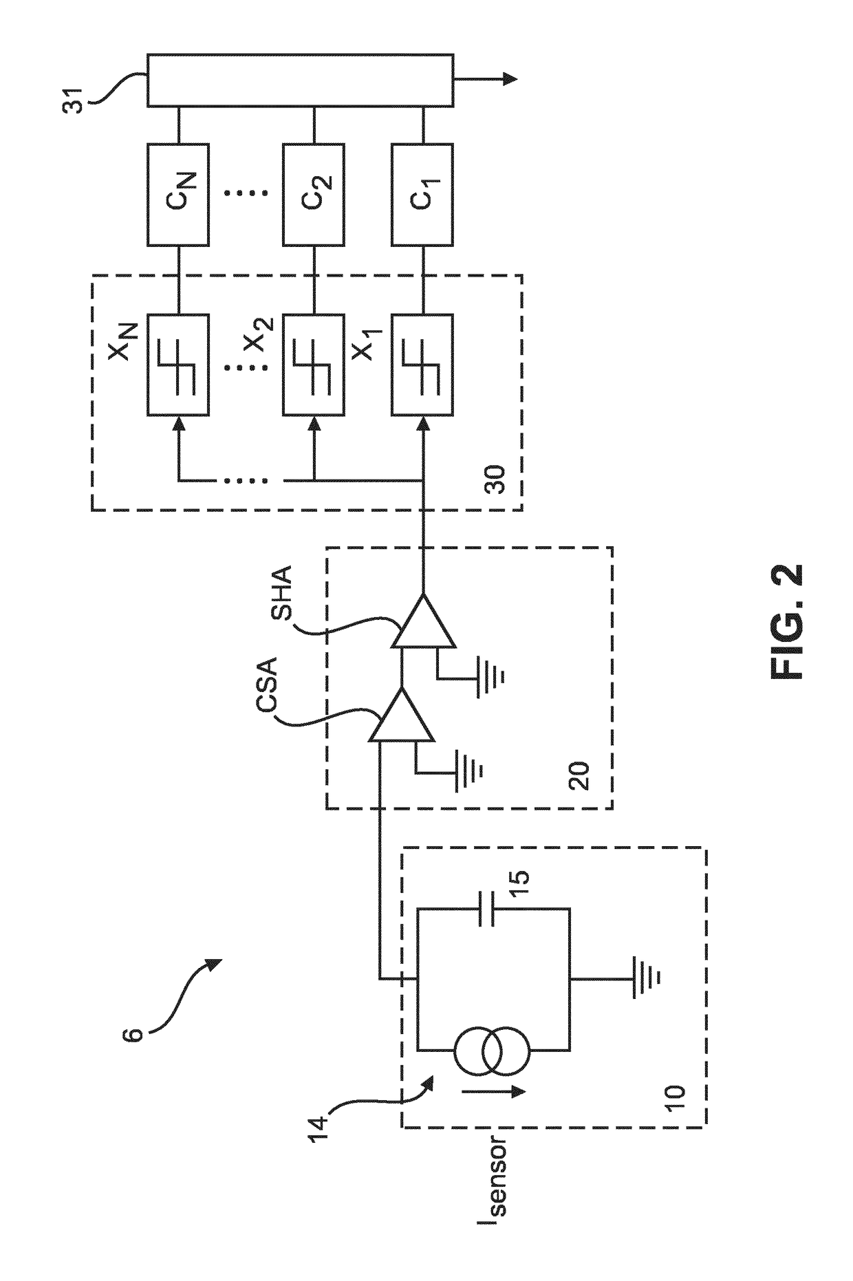
[0111]The use of cadmium zinc telluride (CZT) in spectral computed tomography (CT) applications requires mechanisms in order to compensate dynamic background current components, i.e. leakage currents (i.e. dark currents) and persistent currents caused by photoconductive gain PCG>1. To this end, for DC coupled readout schemes, baseline restorer circuits (BLR) are introduced to detect shifts of the baseline (BL) level at the output of the shaping element and inject / pull a current to correct for the aforementioned shift.

[0112]Baseline restorer circuits are typically implemented by using a peak detector that senses the baseline, a low pass filter (e.g. an integrator) to restrict to the compensation of low frequency BL shifts and (a) transconductor element(s) in charge of injecting or sinking a compensat...


PUM


Abstract

The present invention relates to a detection device (6) for detecting photons emitted by a radiation source (2). The detection device (6) is configured to detect the photons during a first time period. The detection device (6) comprises a sensor (10) having an intermediate direct conversion material for converting photons into electrons and holes, a shaping element (20), and a compensation unit (450, INT, 950). The compensation unit (450, INT, 950) is adapted to provide a compensation signal based on the electrical pulse and on a photoconductive gain of said sensor (10). The core of the invention is to provide circuits to reduce artifacts due to inherent errors with direct conversion detectors in spectral computed tomography by determining a compensation current, by detecting or monitoring a baseline restorer feedback signal, or by ignoring signals above the baseline level.

Description

CROSS REFERENCE TO RELATED APPLICATIONS[0001]This application is the U.S. National Phase application under 35 U.S.C. §371 of International Application No. PCT / EP2014 / 075065, filed Nov. 20, 2014, published as WO 2015 / 078753 on Jun. 4, 2015, which claims the benefit of European Patent Application Number 13194618.8 filed Nov. 27, 2013. These applications are hereby incorporated by reference herein.FIELD OF THE INVENTION[0002]The invention relates to a detection device and a detection method for detecting photons emitted by a radiation source.BACKGROUND OF THE INVENTION[0003]If Cd[Zn]Te with not fully blocking (cathode) contacts is used for single photon counting detectors, the photoconductive gain causes a major problem especially for DC coupled readout electronics: Since it is a slowly changing current on top of the photocurrent, it causes a baseline shift at the output of the analog readout channel towards the set energy thresholds so that, without any correction means, the energies ...

Claims


Application Information

Patent Timeline
Patent Type & Authority Patents(United States)
IPC IPC(8): G01T1/26G01T1/17G01T1/24
CPCG01T1/247G01T1/17G01T1/249
Inventor DAERR, HEINERHERRMANN, CHRISTOPHBERGNER, FRANKSTEADMAN BOOKER, ROGER
Owner KONINKLJIJKE PHILIPS NV
Why Eureka
Try Eureka