Micro electro mechanical system (MEMS) based wide-band polymer photo-detector

a micro electro mechanical and wide-band technology, applied in the field of polymer photodetectors, can solve the problems of limited applicability, low quantum efficiency, and operation within visible waveband and near infrared

Inactive Publication Date: 2017-10-10
INDIAN INSTITUTE OF TECHNOLOGY BOMBAY
View PDF12 Cites 0 Cited by
  • Summary
  • Abstract
  • Description
  • Claims
  • Application Information

AI Technical Summary

Benefits of technology

[0009]It is another object of the present disclosure to provide a simple deposition technique for the polymer photo-detector device without multiple layer stacks, with a low-cost fabrication process.
[0013]An embodiment of the present disclosure discloses a single polymer photo-detector device having wideband spectrum responsivity. To achieve the spectrum responsivity in different wavebands, different dominating properties of different electromagnetic regions of those wavebands are required to be merged on a single device. The current disclosure presents a novel MEMS based photo-detector device wherein the photo-detection capability of the polymer is extended to multiple wavebands, from Ultraviolet, Visible to Infra-red by changing the nano-morphology of the single photoactive layer on a low thermal mass device structure. The photoconductivity and pyroelectric properties of the photoactive material are merged by changing the nano-morphology of the photoactive layer. In an embodiment, the polymer used as the photoactive layer is Polyvinyl Alcohol (PVA), which has excellent capabilities of easy synthesis, low cost, flexible fabrication on different substrates, long term stability, bio-compatibility, and its distinct characteristics include photoconductivity and pyroelectricity.
[0015]A novel feature of the invention is the development of a miniaturized MEMS based single photoactive layer photoconductive polymer on a low thermal mass platform with photoresponsitivity spanning from Ultraviolet, Visible to Infra-red. There is no additional buffer layer for accepting Ultraviolet, visible and Infrared radiation as well as buffer layer to block the charge carrier injection. The fabricated photo-detector is a miniaturized MEMS device which has the potential to be integrated in any lab-on-a-chip system, particularly useful in micro-fluidic and biological sensing. The low thermal mass of the MEMS based structure reduces the effect of localized heating due to Infrared radiation, thereby increasing responsivity of the photo-detector.
[0018]In UV-visible region the photoconductivity is achieved through primary charge carrier excitons, and in Infrared region the vibrational spectroscopy is achieved using pyroelectric properties of the photoactive PVA polymer. The photo-detector exhibited maximum responsivity of 0.53 A / W at 240 nW of power and maximum detection ability of 3.172×10¹² Jones at 470 nm wavelength with 240 nW of power. The minimum response time of 500 ns was observed when excited with 7 ns pulsed laser. The MEMS based photo-detector relaxes the necessity of using different photo-detectors for different wavebands and is acceptable for developing lab-on-chip systems.

Problems solved by technology

Traditional silicon photo-detectors absorb only below 1.1 μm, which means that they can only be operated within visible waveband and Near Infrared, hence having limited applicability.
Further, the aging of device and radiation effects further lower its Quantum efficiency.
The multiple layers make the device bulky as well as expensive.
The multiple layers decrease the cost effectiveness of the photodetector.

Method used


Image

  • Micro electro mechanical system (MEMS) based wide-band polymer photo-detector
  • Micro electro mechanical system (MEMS) based wide-band polymer photo-detector
  • Micro electro mechanical system (MEMS) based wide-band polymer photo-detector

Examples


Embodiment Construction

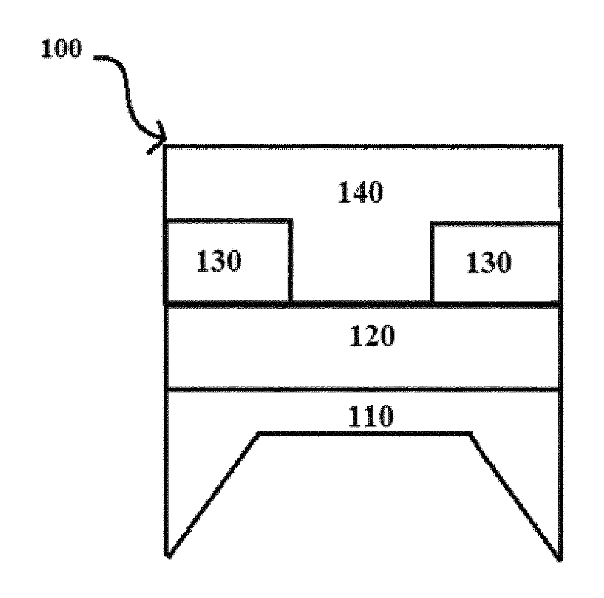
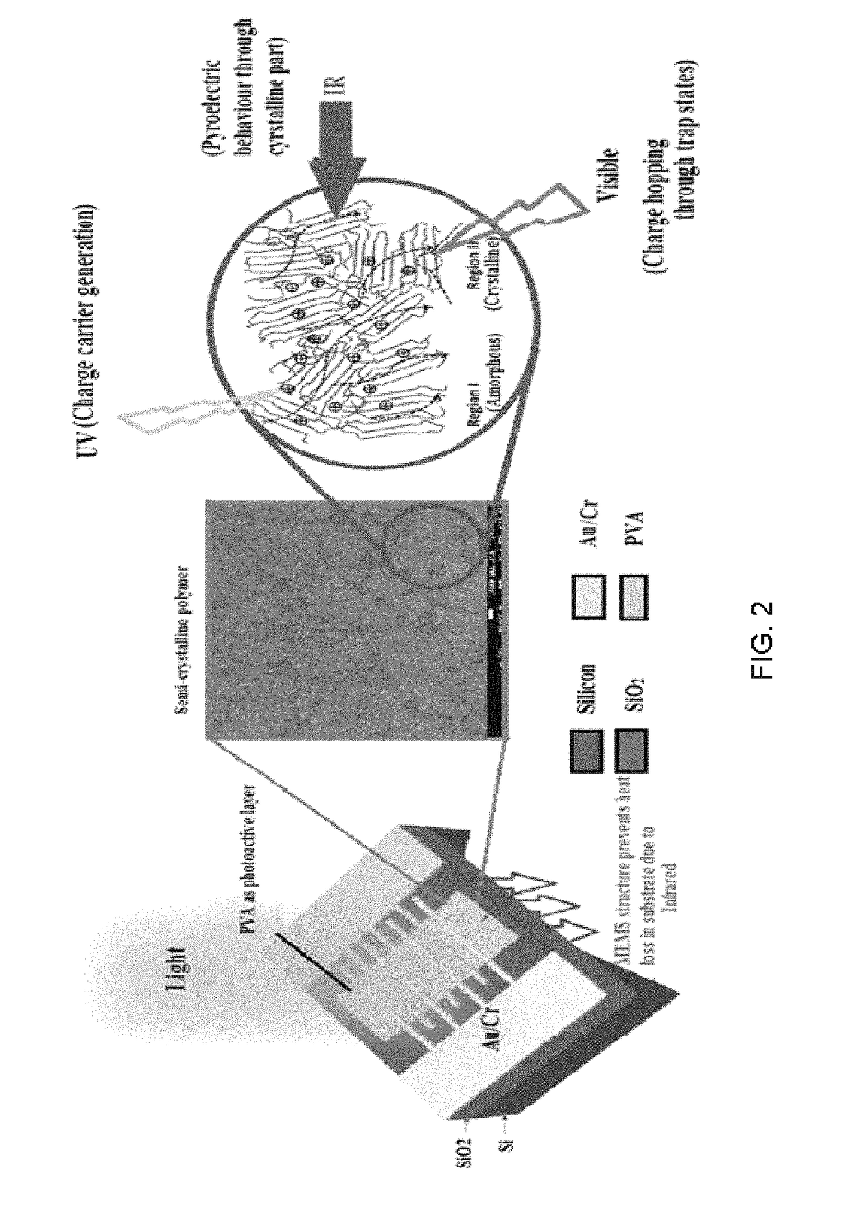
[0025]The present disclosure relates to a polymer photo-detector comprising a single photoactive Polyvinyl Alcohol (PVA) polymer layer having wideband (Ultraviolet-Visible to Infra-red) photo-detection as well as photoconductive and pyroelectric capability. The following description with reference to accompanying drawings is presented to enable one of ordinary skill in the art to make and use the invention and is provided in the context of patent application and its requirements.

[0026]As illustrated in FIG. 1, according to an embodiment, a MEMS based photo-detector device 100 includes a Silicon substrate 110 (a p-type or n-type substrate); an insulating SiO2 layer 120; and a single photoactive Polyvinyl Alcohol (PVA) layer 140 between metal electrodes of Gold 130. The photo-detector is illuminated in the Ultraviolet-Visible light, and charge carriers (singlet excitons, Polarons, and Polaron pairs) are produced in the polymer film. The Exciton generation mechanism is not dominant und...


PUM

PropertyMeasurementUnit
thicknessaaaaaaaaaa
responsivityaaaaaaaaaa
response timeaaaaaaaaaa

Abstract

A polymer based photo-detector has photoresponsivity in Ultraviolet, Visible, Near and Mid Infrared regions. The photo-detector comprises a single layer of polyvinyl alcohol (PVA) as a photoactive layer; with no additional buffer layer for accepting Ultraviolet, Visible and Infrared radiation as well as no buffer layer to block charge carrier injection. The PVA layer's photoresponsivity is extended from Ultraviolet to Near Infrared by changing its nano-morphology on a low thermal device structure. The primarily photo-generated charge carriers diffuse through the amorphous part of the polymer layer and split into charge carriers on the electrodes or by the charge traps in the layer. The charge carrier generation is in the picosecond range; thus the exciton and Polaron drift diffusion cause electrical conduction of the polymer layer under Ultraviolet illumination. The low thermal mass of the MEMS based structure reduces localized heating effect due to Infrared radiation, increasing responsivity of the photo-detector.

Description

CROSS REFERENCE TO RELATED APPLICATIONS[0001]This application claims priority to Indian Patent Application No. 4235 / MUM / 2014, filed Dec. 30, 2014, the entire contents of which is hereby incorporated by reference herein.FIELD OF INVENTION[0002]The present invention relates generally to a polymer photo-detector and, more specifically, to a micro electro mechanical system (MEMS) based photo-detector comprising a single photoactive layer with wide-band (Ultra Violet, Visible to Infrared) photo detection having photoconductive and pyroelectric measurement capability.BACKGROUND[0003]Polymer photo-detectors are sought after for the purpose of photo-detection and measurement of photoconductivity and pyroelectric characteristics due to their low-cost and simple fabrication capability. Traditional silicon photo-detectors absorb only below 1.1 μm, which means that they can only be operated within visible waveband and Near Infrared, hence having limited applicability. Further, the aging of devi...

Claims


Application Information

Patent Timeline
Patent Type & Authority Patents(United States)
IPC IPC(8): H01L51/42H01L51/00
CPCH01L51/4206Y02E10/549H01L51/004H01L51/002H10K71/30H10K85/141H10K30/451
Inventor ROY, SANGITA CHAKIKUNDU, TAPANENDURAO, V. RAMGOPAL
Owner INDIAN INSTITUTE OF TECHNOLOGY BOMBAY
Why Eureka
Try Eureka