Method of forming a metal-insulator-metal capacitor

a metal-insulator and capacitor technology, applied in the field of capacitors, can solve the problems of increasing the leakage current in the device, affecting the overall capacitance, and the use of polycrystalline silicon is difficult, so as to improve the electrical characteristics, and improve the effect of electrical characteristics

Inactive Publication Date: 2006-03-28
SAMSUNG ELECTRONICS CO LTD
View PDF30 Cites 31 Cited by
  • Summary
  • Abstract
  • Description
  • Claims
  • Application Information

AI Technical Summary

Benefits of technology

[0019]The dielectric film can have improved electrical characteristics by undergoing a thermal treatment or plasma process immediately after the dielectric film is formed or after an upper electrode is formed.
[0020]Also, the dielectric film can be formed in multiple steps by repeating deposition and thermal treatment or plasma processing for improving the electrical characteristics.
[0021]After the step of forming a lower electrode, a reaction prevention film can be formed to prevent the reaction between the material of the lower electrode and that of the dielectric film. Preferably, the reaction prevention film is formed by depositing one among the above-mentioned materials to be in an amorphous state. It is also preferable that, when a reaction prevention film is formed, thermal treatment for crystalizing the dielectric film is further performed after an upper electrode is formed.
[0022]According to the present invention, as described above, a refractory metal, which is relatively easy to deposit and pattern, or a conductive compound including a refractory metal, is used to form a lower electrode, and a platinum-family metal or a platinum-family metal oxide, the electrical properties of which is suited for a high dielectric material, is used to form an upper electrode. Thus, a capacitor, which satisfies many characteristics such as a negligible leakage current, high capacitance and the suitability for mass production, can be obtained.

Problems solved by technology

In the case where a material having a high dielectric constant, for example, Ta2O5 or BST((Ba,Sr))TiO3), is used as the dielectric film, it is difficult to use polycrystalline silicon, which is used as an electrode material in the prior art, to form an electrode, since a reduction in the thickness of a dielectric film causes tunneling, thereby increasing leakage current in the device.
However, this method results in degradation in the total capacitance.
However, in a TiN / Ta2O5 / TiN capacitor, the material, TiN, of upper and lower electrodes reacts with the Ta2O5 layer of the dielectric film when they are deposited or when they undergo a subsequent thermal treatment, resulting in deterioration of capacitor characteristics.
However, this also leads to a degradation in the capacitance and results in a rather complicated manufacturing process.
In a Pt / Ta2O5 / Pt capacitor, there are no reactions between the dielectric film and upper and lower electrodes, but the use of a Pt-family metal is relatively expensive.
In particular, deposition techniques providing a good step coverage necessary for forming an electrode in a three-dimensional shape, and simple etching techniques to achieve patterning at a low cost are not put into practical use, so that they are inadequate for mass production.

Method used


Image

  • Method of forming a metal-insulator-metal capacitor
  • Method of forming a metal-insulator-metal capacitor
  • Method of forming a metal-insulator-metal capacitor

Examples


Embodiment Construction

[0030]Hereinafter, embodiments of the present invention will be described in detail with reference to the attached drawings. However, the embodiments of the present invention can be modified into various other forms, and the scope of the present invention must not be interpreted as being restricted to the embodiments. The embodiments are provided to more completely explain the present invention to those skilled in the art. In the drawings, the thicknesses of layers or regions are exaggerated for clarity. Like reference numerals in the drawings denote the same members. Also, when it is written that a layer (film) is formed “on” another layer (film) or a substrate, the layer (film) can be formed directly on the other layer (film) or the substrate, or other layers (films) can intervene therebetween.

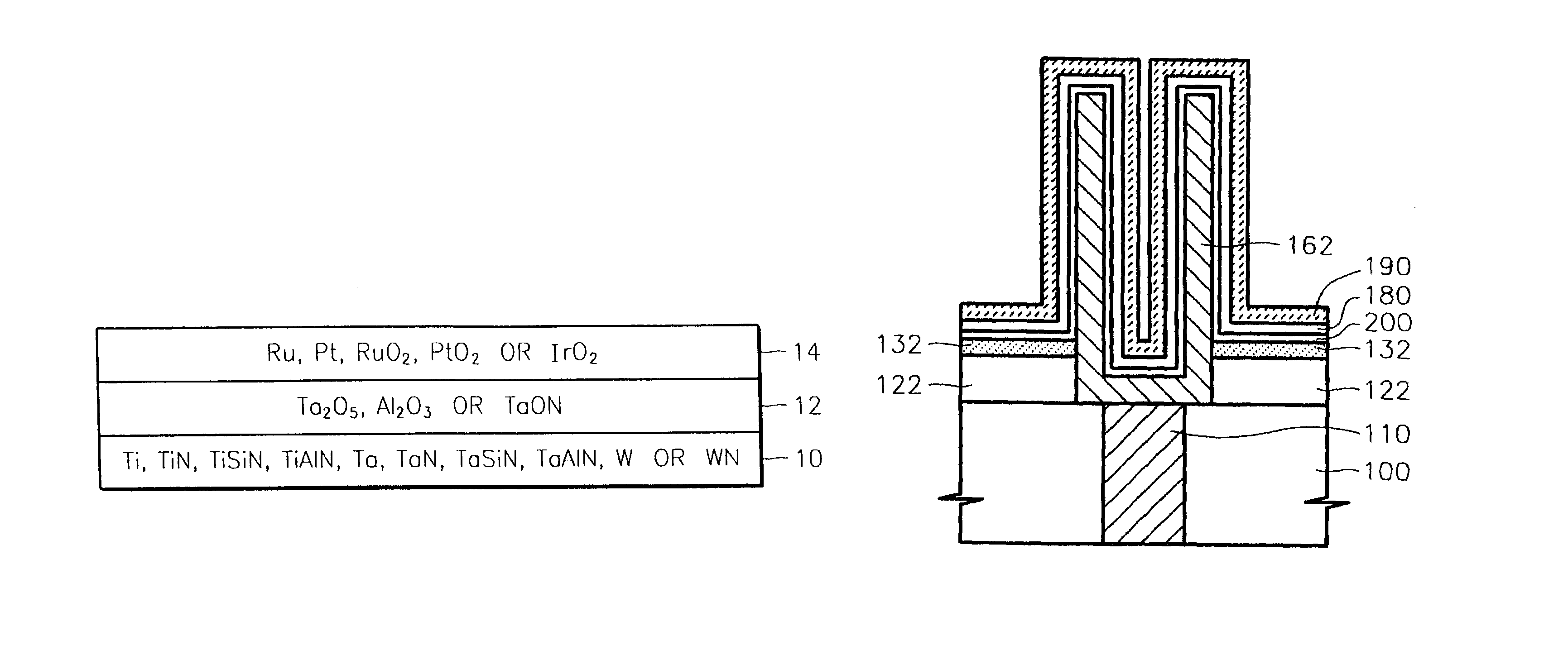
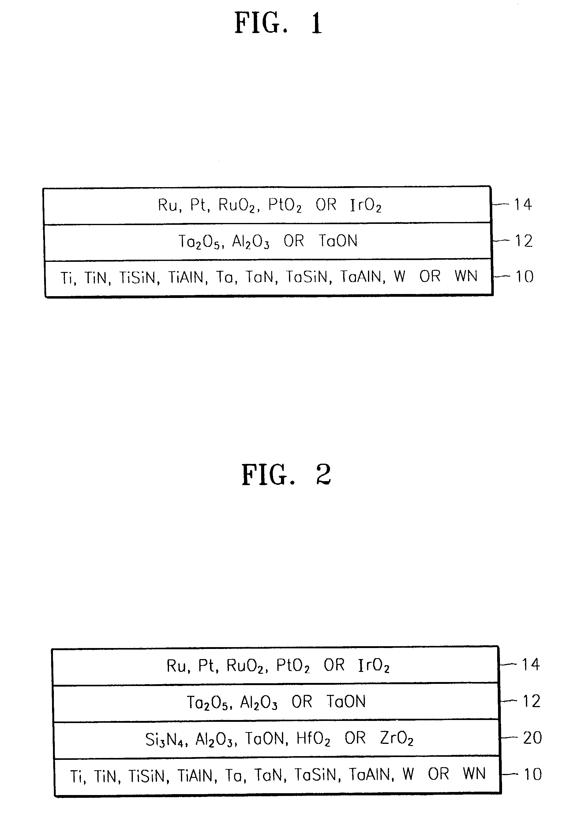
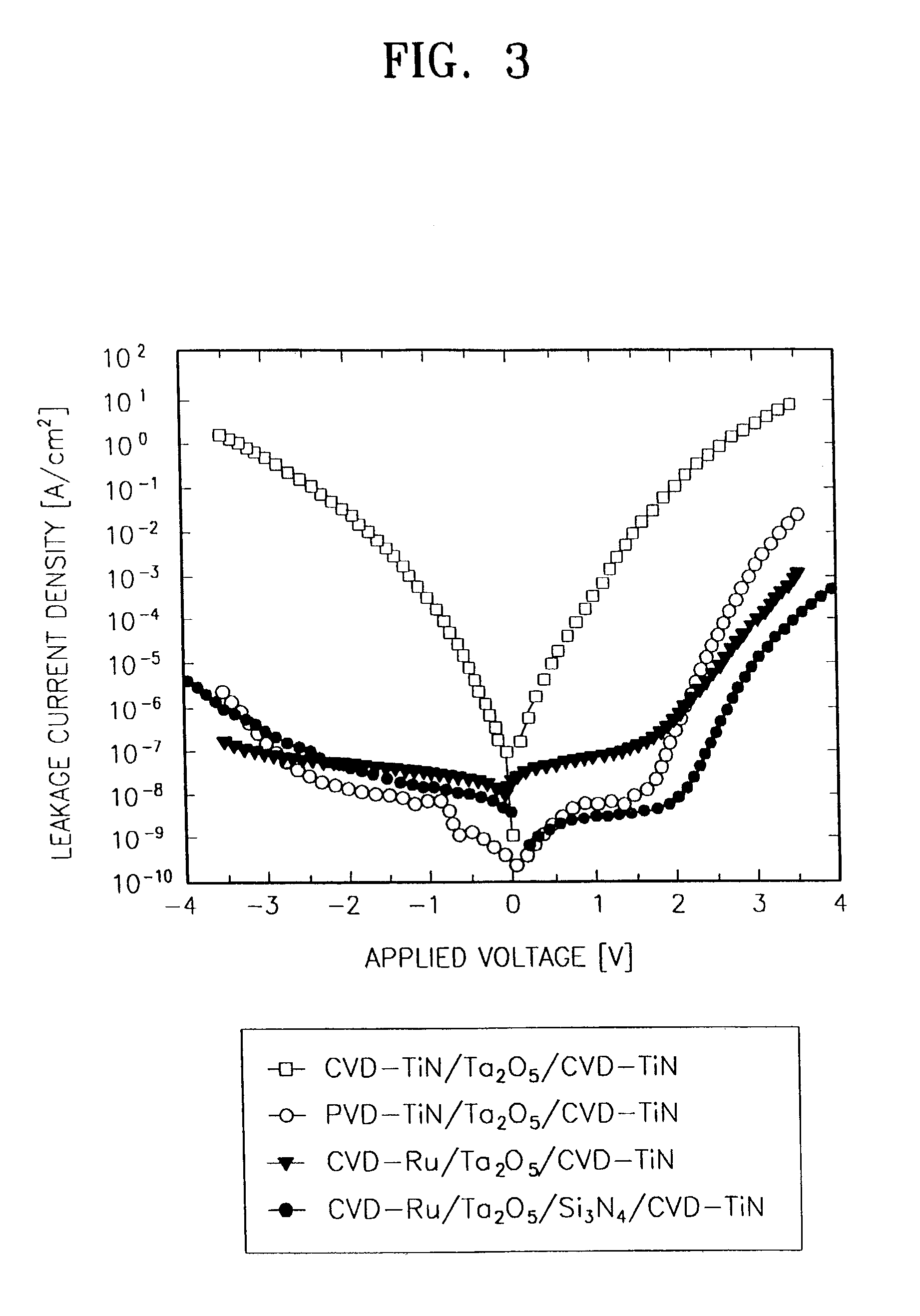
[0031]FIG. 1 conceptually shows the structure of electrodes and a dielectric film according to an embodiment of the present invention. A capacitor according to the present invention shown in...


PUM

PropertyMeasurementUnit
temperatureaaaaaaaaaa
pressureaaaaaaaaaa

Abstract

A metal-insulator-metal (MIM) capacitor of a semiconductor device, and a manufacturing method thereof, includes a lower electrode formed of a refractory metal or a conductive compound including the refractory metal, a dielectric film formed of a high dielectric material, and an upper electrode formed of a platinum-family metal or a platinum-family metal oxide. Accordingly, the MIM capacitor satisfies the criteria of step coverage, electrical characteristics and manufacturing costs, as compared to a conventional MIM capacitor in which the upper and lower electrodes are formed of the same material such as a platinum-family metal, a refractory metal or a conductive compound including the refractory metal. The capacitor is especially suitable for mass production in semiconductor fabrication processes.

Description

RELATED APPLICATIONS[0001]This application is a divisional application of U.S. Ser. No. 09 / 863,679, filed May 23, 2001, the content of which is incorporated herein by reference.BACKGROUND OF THE INVENTION[0002]1. Field of the Invention[0003]The present invention relates to a capacitor for a semiconductor device and a manufacturing method thereof, and more particularly, to a capacitor having a metal-insulator-metal structure (hereinafter, referred to as a MIM capacitor) and a manufacturing method thereof.[0004]2. Description of the Related Art[0005]As semiconductor technology evolves, the area occupied by each device on a chip gradually decreases due to an increase in integration density. Such devices include capacitors, which for example are responsible for storing information on a dynamic random access memory (DRAM). Capacitors are required to maintain large capacitance values, even though integration requires there area to continue to decrease.[0006]A number of methods have been p...

Claims


Application Information

Patent Timeline
Patent Type & Authority Patents(United States)
IPC IPC(8): H01L21/302H01L21/8242H01L21/02H01L21/316
CPCH01L28/91H01L21/31604H01L21/0228H01L21/02183H10B12/00H01L21/02337H01L21/02348
Inventor KIM, WAN-DONKIM, JIN-WONWON, SEOK-JUNYOO, CHA-YOUNG
Owner SAMSUNG ELECTRONICS CO LTD
Why Eureka
Try Eureka