Light emitting diode chip, and methods for manufacturing and packaging the same

Active Publication Date: 2010-08-19
LITE ON TECH CORP +1
View PDF4 Cites 29 Cited by
  • Summary
  • Abstract
  • Description
  • Claims
  • Application Information

AI Technical Summary

Benefits of technology

[0008]According to the present invention, a light emitting diode chip is provided with two inclined sidewalls on two sides thereof. Due to the inclined sidewalls, it is easy to deposit the conductive portions evenly on the inclined sidewalls, thereby avoiding a problem of poor step coverage. Furthermore, with the conductive layers on the inclined sidewalls, connections of the electrodes of the light emitting diode chip can be extended to two sides or the bottom side of the substrate. Such an arrangement facilitates subsequent packaging processes of the light emitting diode chip. Particularly, no wire bonding process is needed in this invention, and the package volume of the light emitting diode chip can be reduced.
[0009]The invention further provides methods of forming a reflective cup and packaging the light emitting diode for system in package or wafer level package. It merely requires one step photolithography process to form a cavity with a reflection layer. Compared to the prior art which requires two steps of photolithography, this invention reduces processing time and production cost. Furthermore, the packaging method of the invention does not need any wire bonding process to form a wiring connection with the package substrate, thereby saving the processing time, enhancing productivity, and reducing the package volume.
[0010]The invention further provides a packaging method in which connections of the electrodes on the light emitting diode chip can be extended to the lower surface of the package substrate without forming a via hole inside the reflective cup, thereby avoiding destruction to the sealing of the light emitting diode chip, and eliminating the problems of the prior art in that the chip is susceptible to moisture and the package structure is likely to be fragile due to the via hole in the reflective cup used for extending the electrode to a bottom of the package substrate. In addition, the package structure produced by the invention can be directly mounted on a printed circuit board of an application product without using the wire bonding process. Accordingly, the yield of defective products due to wire breakage can be reduced, the reliability of the package structure can be improved, and assembling of the package structure will be more simplified and more convenient for downstream application processes.
[0011]In the light emitting diode chip of the invention, by virtue of the in

Problems solved by technology

In addition, since wire connections are made one by one using a machine during the wire bonding process, the production efficiency is relatively low and is unfavorable for a system in package or a wafer level package.
However, in the flip chip process, there is a need to deposit plenty of gold bumps on each chip, which is time-consuming and also decreases the packaging process efficiency of

Method used


Image

  • Light emitting diode chip, and methods for manufacturing and packaging the same
  • Light emitting diode chip, and methods for manufacturing and packaging the same
  • Light emitting diode chip, and methods for manufacturing and packaging the same

Examples


first embodiment

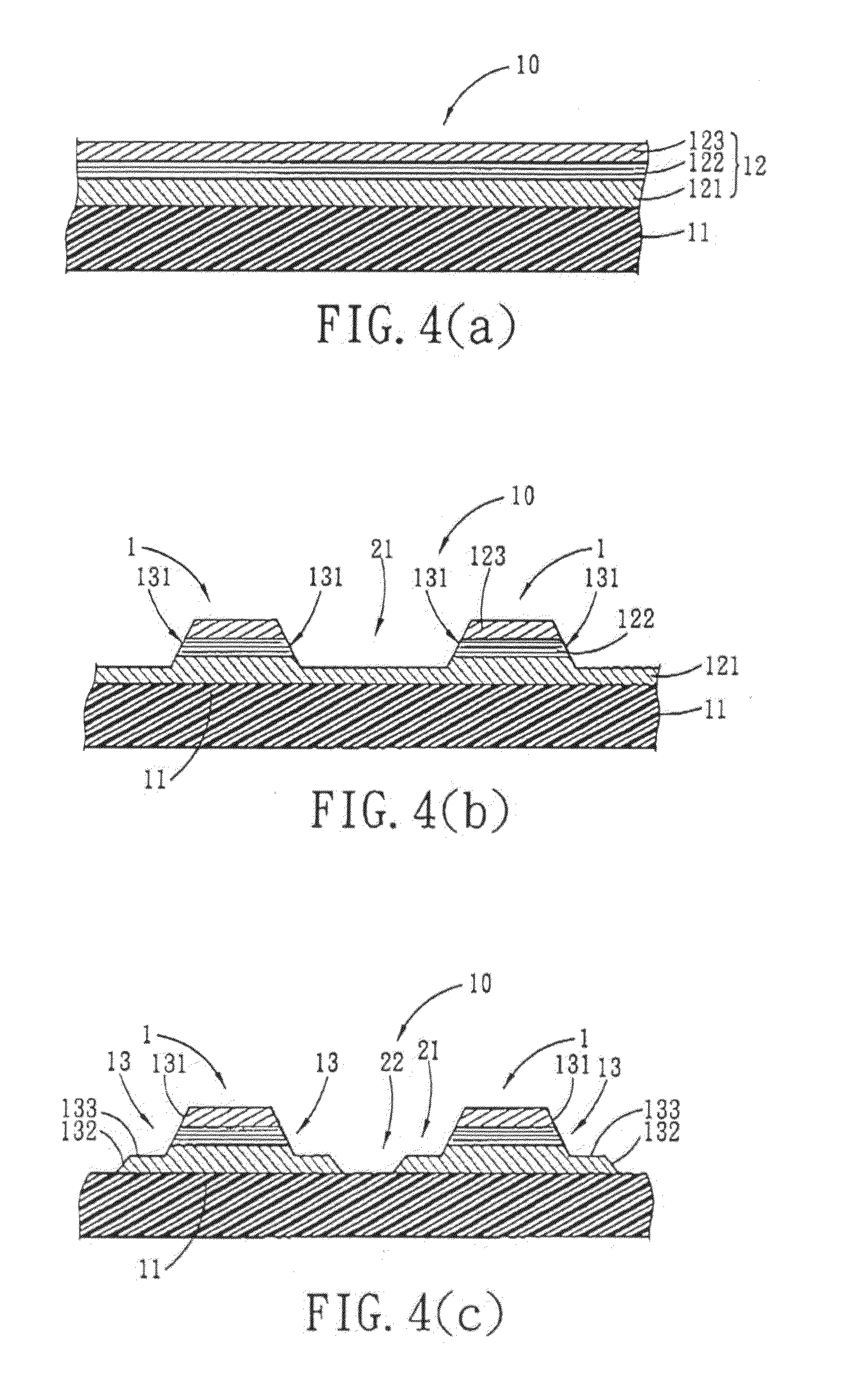
[0030]Referring to FIG. 4 (a) to FIG. 4 (f), the steps included in the method for making the light emitting diode chip 1 according to the present invention are described as follows.

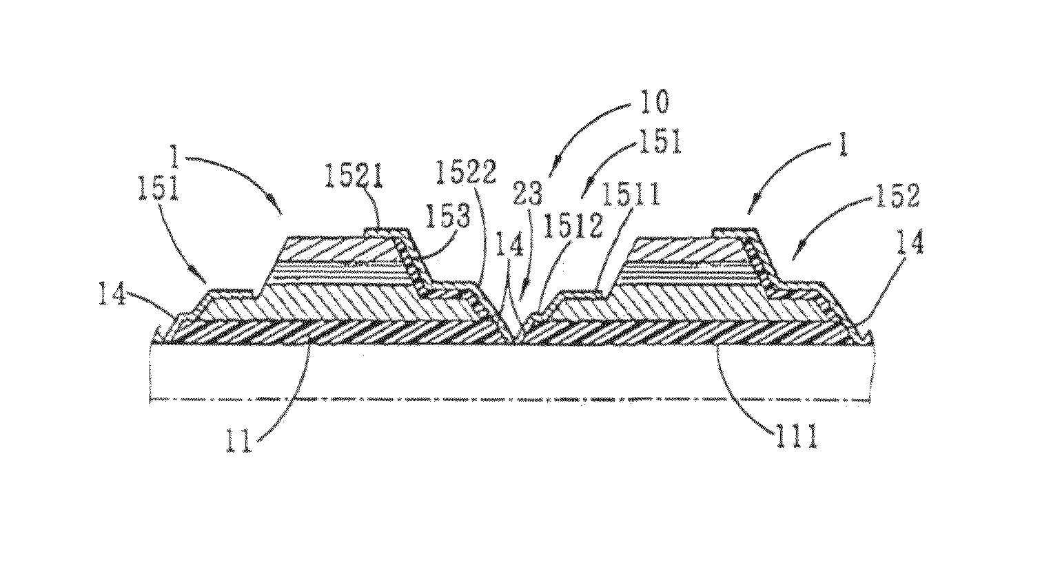
[0031]As shown in FIG. 4 (a), a mother chip 10 formed with an epitaxial structure is provided. The mother chip 10 comprises a substrate 11 and an epitaxial layer 12 formed on the substrate 11. The epitaxial layer 12 includes: a first type semiconductor layer 121 formed on the substrate 11, a light emitting layer 122 formed on the first type semiconductor layer 121, and a second type semiconductor layer 123 formed on the light emitting layer 122. In this embodiment, the substrate 11 is made of sapphire, and has a thickness of approximately 350 μm. The first type semiconductor layer 121 is made of n-GaN, and the second type semiconductor layer 123 is made of p-GaN.

[0032]Using a patterning process of semiconductor processing technologies, a plurality of predetermined chip positions (not shown) and recesses (...

second embodiment

[0053]FIG. 10 (a) to FIG. 10 (c) illustrate steps of the method for packaging the light emitting diode of the second embodiment according to the present invention, which is used for packaging the aforesaid light emitting diode chip 1′.

[0054]As shown in FIG. 10 (a), after predetermined positions (not labeled) of the second conductive portions 1513′, 1523′ on the bottom surface 111′ of the light emitting diode chip 1′ (see FIGS. 8 and 9) are defined in the reflective cup 34′, two conductive extension portions 35′ are formed by a metallization process such that the conductive extension portions 35′ extend to parts of the package substrate 3′ outwardly of the reflective cup 34′ from the predetermined positions of the second conductive portions 1513′, 1523′. In this embodiment, the steps of the method used for making the reflective cup 34′ are the same as those of the first embodiment shown in FIG. 7 (a) to FIG. 7 (d). Because both of the reflective cup 34′ and the package substrate 3′ a...

third embodiment

[0058]FIG. 11 (a) to FIG. 11 (f) illustrate the method for packaging the light emitting diode of the third embodiment according to the present invention.

[0059]As shown in FIG. 11 (a), two protection portions 42 are respectively formed on upper and lower surfaces 411, 412 of the package substrate 41. The protection portions 42 are patterned to form a plurality of through holes 421, 422 predefining cavity locations 421 for the reflective cups 471 (see FIG. 11(c)), and predefining via-hole locations 422 for via holes 44 (see FIG. 11b) on two sides of each of the cavity locations 421. The via-hole locations 422 on the upper and lower surfaces 411, 412 of the package substrate 41 are aligned in a top-to-bottom direction. As shown in FIG. 11 (b), the package substrate 41 is etched by an etching agent through the through hole 421 of the protection portion 42 to form the cavity 43 that prelocates the reflective cup 471 (as shown in FIG. 11 (c)) such that an opening 431 of the cavity 43 is a...


PUM


Abstract

A light emitting diode chip includes a substrate, an epitaxial layer, two inclined plane units, and two electrode units. The substrate has top and bottom surfaces. The epitaxial layer is disposed on the top surface of the substrate. Each of the inclined plane units is inclined downwardly and outwardly from the epitaxial layer toward the bottom surface of the substrate, and includes an inclined sidewall formed on the epitaxial layer, and a substrate inclined wall formed on the substrate. Each of the electrode units includes an electrode disposed on the epitaxial layer, and a conductive portion extending from the electrode to the substrate inclined wall along corresponding one of the inclined plane units.

Description

CROSS-REFERENCE TO RELATED APPLICATION[0001]This application claims priority of Chinese application no. 200910037346.8, filed on Feb. 19, 2009.BACKGROUND OF THE INVENTION[0002]1. Field of the Invention[0003]This invention relates to a light emitting diode chip, which has small package volume and which can be rapidly manufactured, and methods for manufacturing and packaging the light emitting diode chip.[0004]2. Description of the Related Art[0005]As shown in FIG. 1, a conventional light emitting diode chip 91 is electrically connected to external electrodes 93 on a substrate 92 by a wire bonding process. However, a larger space on the substrate 92 is required for the wire bonding process. In addition, since wire connections are made one by one using a machine during the wire bonding process, the production efficiency is relatively low and is unfavorable for a system in package or a wafer level package.[0006]In order to alleviate the problems attributed to the wire bonding process, a...

Claims


Application Information

Patent Timeline
IPC IPC(8): H01L21/28H01L21/50
CPCH01L33/0095H01L33/46H01L33/385H01L33/44H01L33/486H01L33/62H01L2224/48091H01L2224/49107H01L2224/73265H01L2924/3025H01L33/52H01L2924/01087H01L2924/01019H01L2224/32145H01L33/20H01L2924/00014H01L2924/00
Inventor KAO, CHIH-CHIANG
Owner LITE ON TECH CORP
Why Eureka
Try Eureka