

Plasma etching apparatus and plasma etching method
a technology of plasma etching and apparatus, which is applied in the direction of electrical equipment, decorative arts, electric discharge tubes, etc., can solve the problems of insufficient technology and difficulty in performing etching through the operation of faraday shield electrodes, and achieve the effect of suppressing the generation of particles and high manufacturing yield
- Summary
- Abstract
- Description
- Claims
- Application Information
AI Technical Summary
Benefits of technology
Problems solved by technology
Method used
Image

Examples
first embodiment
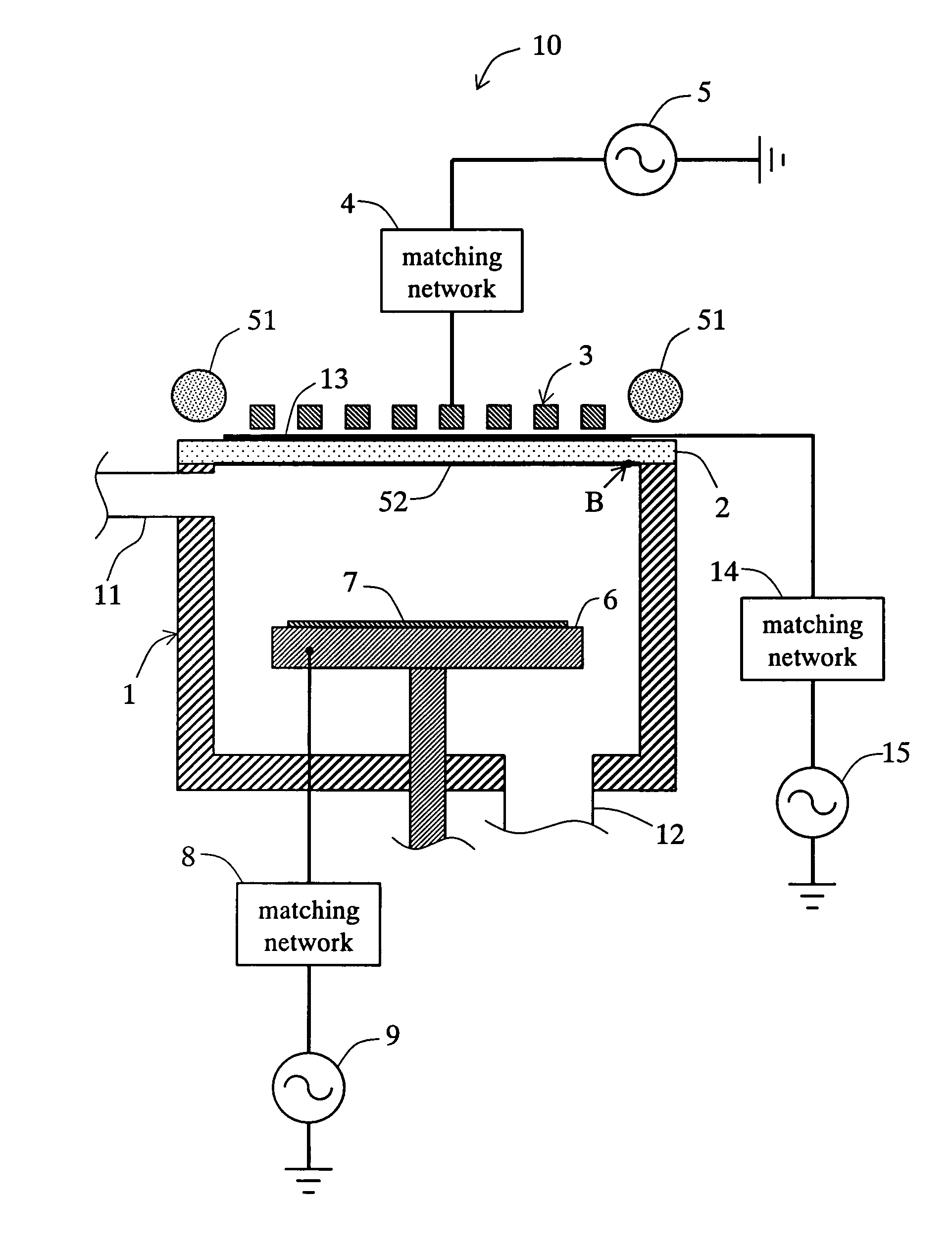
[0043] A detailed description of a plasma etching apparatus and plasma etching method relating to a first embodiment of the present invention is provided hereafter, with reference to the drawings.
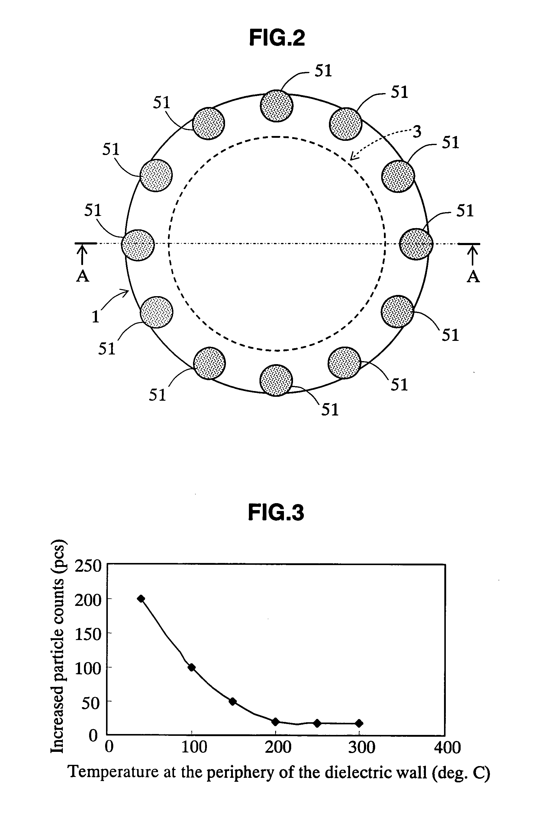
[0044]FIG. 1 is a schematic view showing the plasma etching apparatus relating to the present embodiment. Moreover, FIG. 2 is a schematic top view showing the plasma etching apparatus relating to the present embodiment. In addition, FIG. 1 is a cross-sectional view at the A-A line shown in FIG. 2. Furthermore, in FIG. 2, a flat coil is shown only its outer shape by the broken line.
[0045] As shown in FIG. 1 and FIG. 2, the plasma etching apparatus relating to the present embodiment is provided with a chamber 1 of nearly cylindrical shape having an axis in the vertical direction. The upper wall of the chamber 1 is constructed from, for instance, a plate-shaped dielectric wall 2 consisting of a dielectric material such as quarts. On the upper surface of the dielectric wall 2 is arranged a Fa...
second embodiment
[0060] A detailed description of a plasma etching apparatus and plasma etching method relating to a second embodiment of the present invention is provided hereafter, with reference to the drawings. FIG. 4 is a schematic view showing a plasma etching apparatus relating to the present embodiment. Moreover, FIG. 5 is a schematic top view showing the plasma etching apparatus relating to the present embodiment. In addition, FIG. 4 is a cross-sectional view at the A-A line shown in FIG. 5. Furthermore, in FIG. 5, a flat coil is shown only its outer shape by the broken line.
[0061] The plasma etching apparatus relating to the present embodiment adopts, in lieu of the lamp 51 of the first embodiment, a heater as the heating unit which heats the periphery of the dielectric wall 2. In other words, as shown in FIG. 4 and FIG. 5, the plasma etching apparatus 10 of the present embodiment is provided with a heater 53 such as an electrical resistance heater and the like in the periphery of the die...
third embodiment
[0068] An explanation of the plasma etching apparatus and plasma etching method relating to the third embodiment of the present invention is provided hereafter, with reference to the drawings. FIG. 7 is a schematic view showing the plasma etching apparatus relating to the present embodiment. Moreover, FIG. 8 is a schematic top view showing the plasma etching apparatus relating to the present embodiment. In addition, FIG. 7 is a cross-sectional view at the A-A line shown in FIG. 8. Furthermore, in FIG. 8, a flat coil is shown only its outer shape by the broken line.
[0069] The plasma etching apparatus relating to the present embodiment adopts, in lieu of the heater 53 of the second embodiment, a high-frequency power absorber 54 made of absorption material of the high-frequency power as the heating unit. In other words, as shown in FIG. 7 and FIG. 8, the plasma etching apparatus 10 of the present embodiment comprise the dielectric wall 2 of which the periphery is composed of the high-...
PUM
| Property | Measurement | Unit |
|---|---|---|
| Temperature | aaaaa | aaaaa |
| Dielectric polarization enthalpy | aaaaa | aaaaa |
| Magnetic field | aaaaa | aaaaa |
Abstract
Description
Claims
Application Information