Supercharge Your Innovation With Domain-Expert AI Agents!

Illumination system of a microlithographic projection exposure apparatus

a technology of exposure apparatus and illumination system, which is applied in the direction of microlithography exposure apparatus, printers, instruments, etc., can solve the problems of light loss, difficult to finally adjust the illumination setting, and need for replacement of the setting

Active Publication Date: 2017-10-31
CARL ZEISS SMT GMBH
View PDF42 Cites 1 Cited by
  • Summary
  • Abstract
  • Description
  • Claims
  • Application Information

AI Technical Summary

Benefits of technology

The present invention provides an illumination system for a microlithographic projection exposure apparatus that can vary the geometry of the illuminated field and produce different field dependencies of the angular light distribution at the mask plane. This enables a smooth transition between different angular irradiance distributions and allows for fine adjustments of field dependency to improve imaging quality. The illumination system includes a spatial light modulator to achieve sharp and abrupt transitions between different angular irradiance distributions. The method of operating the illumination system allows for the adjustment of the field geometry and defines the light pattern of the light entrance facets more sharply.

Problems solved by technology

However, any change of the illumination setting requires a replacement of the stop.
This makes it difficult to finally adjust the illumination setting, because this would require a very large number of stops that have aperture(s) with slightly different sizes, shapes or locations.
Furthermore, the use of stops inevitably results in light losses which reduces the throughput of the apparatus.

Method used


Image

  • Illumination system of a microlithographic projection exposure apparatus
  • Illumination system of a microlithographic projection exposure apparatus
  • Illumination system of a microlithographic projection exposure apparatus

Examples


Embodiment Construction

I. General Construction of Projection Exposure Apparatus

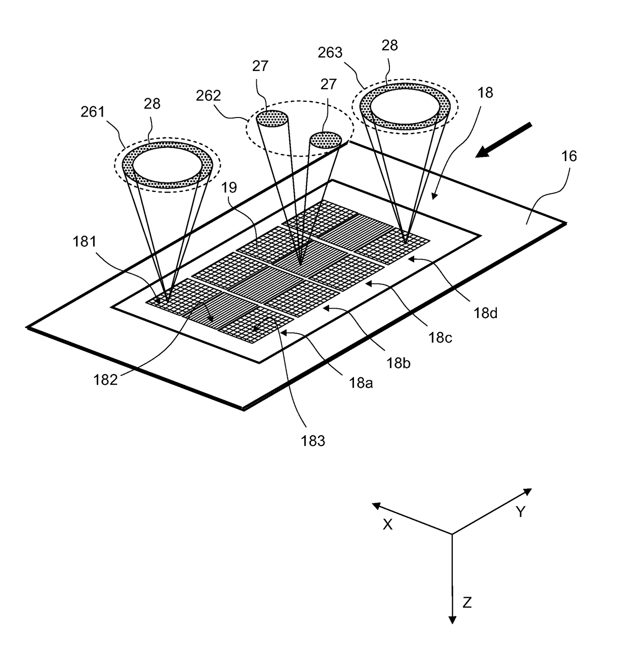
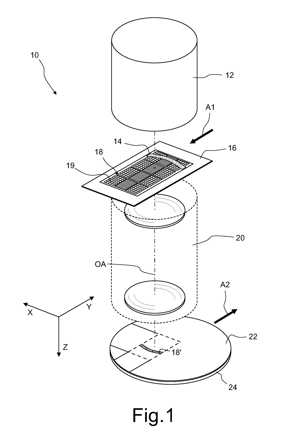
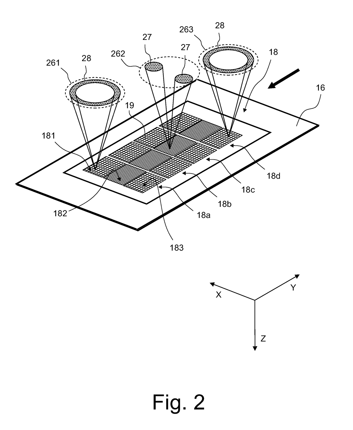
[0074]FIG. 1 is a perspective and highly simplified view of a projection exposure apparatus 10 in accordance with the present invention. The apparatus 10 comprises an illumination system 12 which produces a projection light beam. The latter illuminates a field 14 on a mask 16 containing a pattern 18 formed by a plurality of small features 19 that are schematically indicated in FIG. 1 as thin lines. In this embodiment the illuminated field 14 has the shape of a ring segment. However, other shapes of the illuminated field 14, for example rectangles, are contemplated as well.

[0075]A projection objective 20 images the pattern 18 within the illuminated field 14 onto a light sensitive layer 22, for example a photoresist, which is supported by a substrate 24. The substrate 24, which may be formed by a silicon wafer, is arranged on a wafer stage (not shown) such that a top surface of the light sensitive layer 22 is precisely located in...


PUM

PropertyMeasurementUnit
wavelengthaaaaaaaaaa
wavelengthsaaaaaaaaaa
diameteraaaaaaaaaa

Abstract

An illumination system of a microlithographic projection exposure apparatus comprises an optical integrator having a plurality of light entrance facets and a beam deflection array of reflective or transparent beam deflecting elements. Each beam deflecting element is configured to illuminate a spot on the optical integrator at a position that is variable by changing a deflection angle produced by the beam deflecting element. The illumination system further comprises a control unit which is configured to control the beam deflection elements in such a manner that a light pattern assembled from the spots on at least one of the light entrance facets is varied in response to an input command that a field dependency of the angular irradiance distribution in a mask plane shall be modified.

Description

FIELD OF THE INVENTION[0001]The invention generally relates to illumination systems for illuminating a mask in microlithographic exposure apparatus, and in particular to such systems comprising an array of mirrors or other beam deflecting elements to define the irradiance distribution in a pupil plane. The invention also relates to a method of operating such illumination systems.DESCRIPTION OF RELATED ART[0002]Microlithography (also called photolithography or simply lithography) is a technology for the fabrication of integrated circuits, liquid crystal displays and other microstructured devices. The process of microlithography, in conjunction with the process of etching, is used to pattern features in thin film stacks that have been formed on a substrate, for example a silicon wafer. At each layer of the fabrication, the wafer is first coated with a photoresist which is a material that is sensitive to radiation, such as deep ultraviolet (DUV) light. Next, the wafer with the photores...

Claims


Application Information

Patent Timeline
Patent Type & Authority Patents(United States)
IPC IPC(8): G03B27/72G03B27/54G03F7/20
CPCG03F7/70116G03F7/70191G03F7/70083G03F7/70075
Inventor DEGUENTHER, MARKUS
Owner CARL ZEISS SMT GMBH
Features
  • R&D
  • Intellectual Property
  • Life Sciences
  • Materials
  • Tech Scout
  • Unparalleled Data Quality
  • Higher Quality Content
  • 60% Fewer Hallucinations
Learn More