Substrate structure and manufacturing method thereof

a technology of substrate structure and manufacturing method, which is applied in the direction of printed circuit aspects, printed circuit non-printed electric components association, basic electric elements, etc., can solve the problems of high cost of fiberglass substrate structure, high cost of fiberglass substrate, and difficulty in laser drilling of substrate containing fiberglass, etc., to achieve high electric characteristics, improve electrical properties and signal stability, and neat dissipation

Active Publication Date: 2017-10-31
PHOENIX PIONEER TECH
View PDF43 Cites 1 Cited by
  • Summary
  • Abstract
  • Description
  • Claims
  • Application Information

AI Technical Summary

Benefits of technology

[0014]According to the above description, the substrate structure and manufacturing method of the present invention use a substrate containing metal material instead of fiberglass. Meanwhile, a simple manufacturing process instead of forming blind holes and through holes by laser drilling and mechanical drilling is used to form a metal core layer, conductive pillar layer, and a conductive wiring layer. Accordingly, the substrate structure and manufacturing method of the present invention achieve the fine line spacing to narrow a size of a substrate, and increase the electrical property and signal stability to meet high electric characteristics with rigidity and neat dissipation. Therefore, the processing time and cost of the substrate structure will be significantly reduced.

Problems solved by technology

However, fiberglass is generally used in the thin substrate structure with high cost.
Rigidity and heat dissipation of fiberglass is not as metal material, such that the substrate containing fiberglass is often prone to warpage.
Laser drilling of the substrate containing fiberglass is more difficult, such that the holes drilled by laser are poor and unable to meet the requirement of fine line spacing.
Also, it needs complex process and a long processing time to form a stacked structure with blind holes by laser drilling.
Therefore, the substrate containing fiberglass does not have industrial advantages.
Thus, the complexity of the manufacturing process of the substrate containing metal material increases.
In addition, laser drilling and mechanical drilling are simultaneously used to form blind holes and through holes in the same layer of the substrate containing metal material, such that the offset generated by registration errors is unable to racer the requirement of fine line spacing.

Method used


Image

  • Substrate structure and manufacturing method thereof
  • Substrate structure and manufacturing method thereof
  • Substrate structure and manufacturing method thereof

Examples


Embodiment Construction

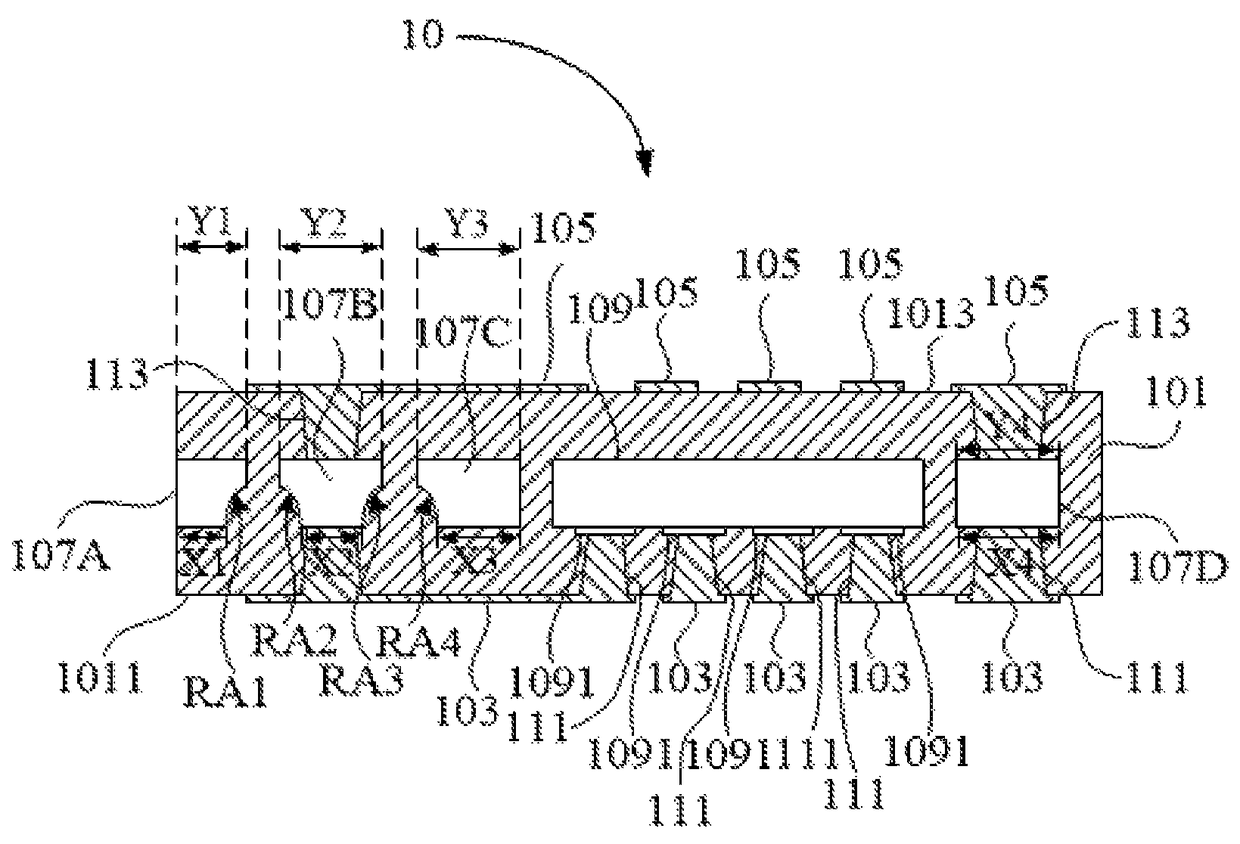
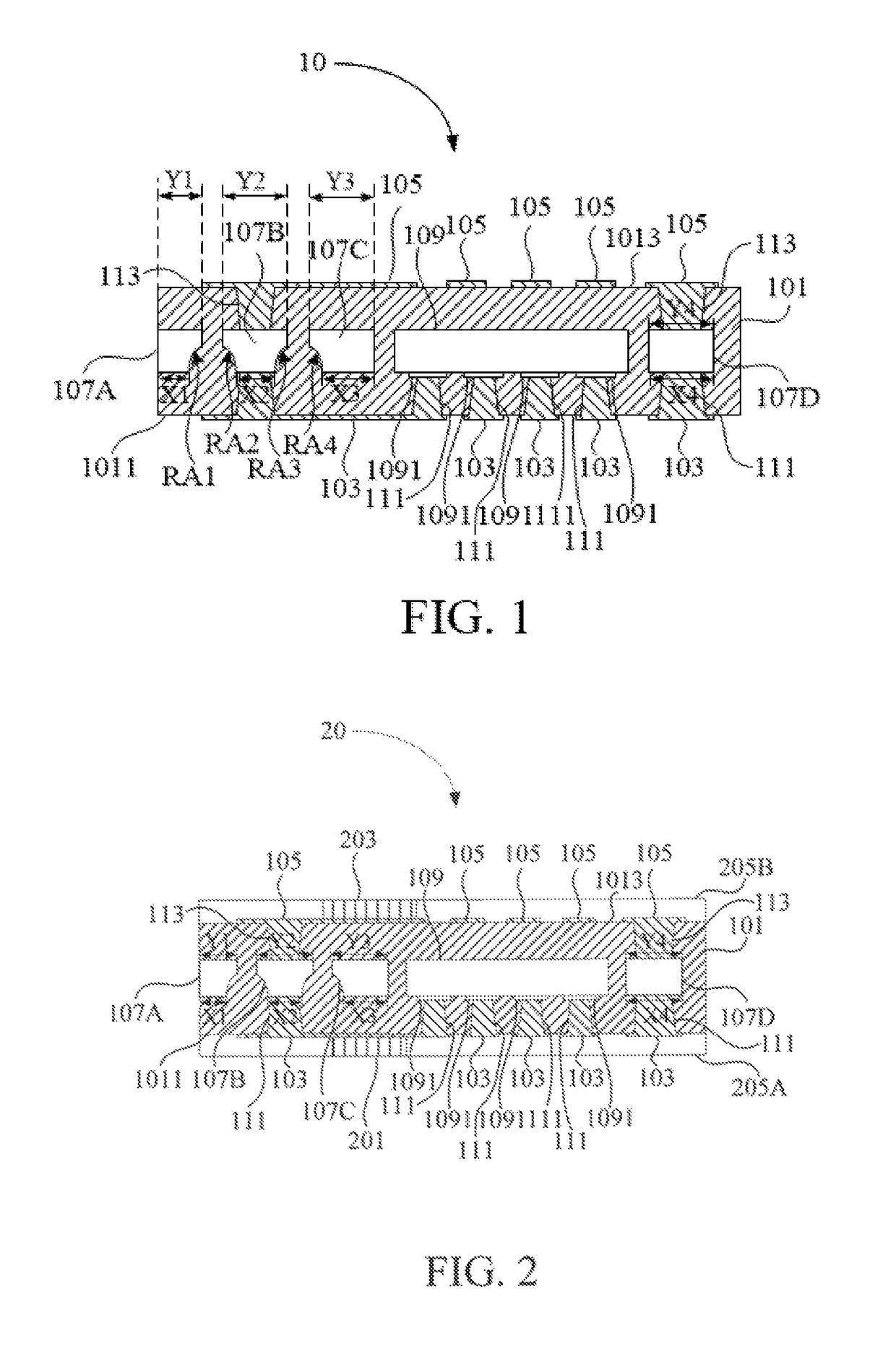
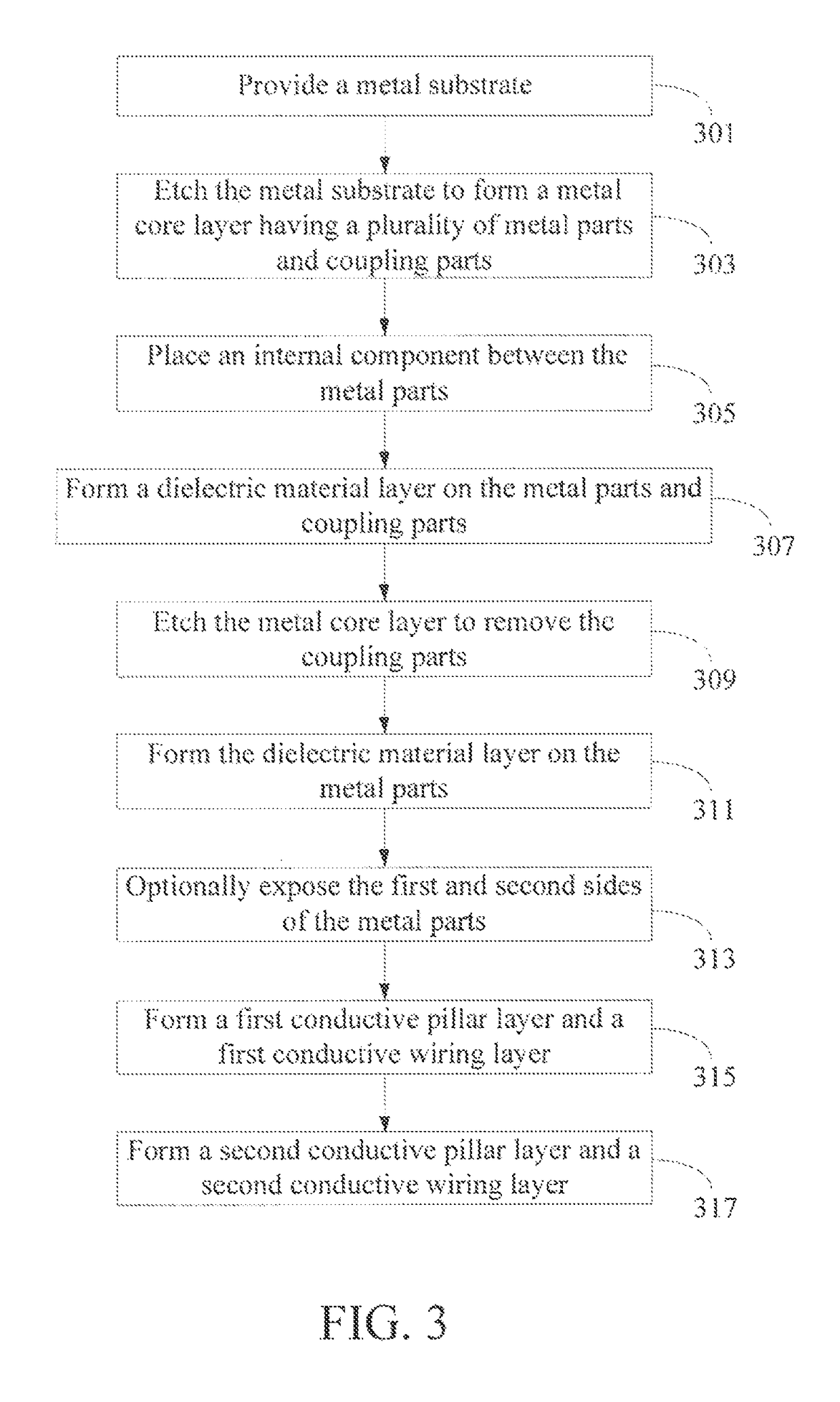
[0023]In the following description, this invention will be explained with reference to embodiments thereof. However, the description of these embodiments is only for purposes of illustration rather than limitation. It should be appreciated that in the following embodiments and attached drawings, elements unrelated to this invention are omitted from depictions; and dimensional relationships among individual elements in the attached drawings are illustrated only for ease of understanding, but not to limit the actual scale.

[0024]FIG. 1 depicts a substrate structure 10 of a first embodiment. The substrate structure 10 comprises a dielectric material layer 101, a first conductive wiring layer 103, a second conductive wiring layer 105, a metal core layer, a first conductive pillar layer 111, a second conductive pillar layer 113, and an internal component 109. The dielectric material layer 101 has a first surface 1011 and a second surface 1013. The metal core layer has four metal parts 107...


PUM

PropertyMeasurementUnit
conductiveaaaaaaaaaa
chamfer angleaaaaaaaaaa
widthaaaaaaaaaa

Abstract

A substrate structure and a manufacturing method thereof are provided. The substrate structure comprises a dielectric material layer, a conductive wiring layer, a metal core layer, and a conductive pillar layer. The conductive wiring layer is disposed on a surface of the dielectric material layer. The metal core layer having a metal part is disposed inside the dielectric material layer. The conductive pillar layer is disposed inside the dielectric material layer and between the metal core layer and the conductive wiring layer. The metal part has a first side and a second side opposite the first side. One of the first side and the second side is electrically connected to the conductive pillar layer. A width of the first side is different from a width of the second side.

Description

[0001]This application claims the benefit of priority based on People's Republic of China Patent Application No 201510413983.6, filed on Jul. 15, 2015, the contents of which are incorporated herein by reference in their entirety.CROSS-REFERENCES TO RELATED APPLICATIONS[0002]Not applicable.BACKGROUND OF THE INVENTION[0003]Field of the Invention[0004]This invention is regarding a substrate structure and a manufacturing method thereof. More precisely speaking, this invention is regarding a semiconductor substrate structure and a manufacturing method thereof.[0005]Descriptions of the Related Art[0006]In recent years, users seek electronic products with compact size, high performance and versatility. Electronics manufacturers must accommodate more components in a limited area of an integrated circuit (IC) to achieve high density and miniaturization. Thus, electronics manufacturers develop a new package of the IC for embedding components in a substrate to reduce the package size and the c...

Claims


Application Information

Patent Timeline
Patent Type & Authority Patents(United States)
IPC IPC(8): H05K1/00H01L21/48H01L23/00H01L23/498H01L23/538H01L23/485H01L23/13H01L21/56H05K1/18
CPCH01L23/13H01L21/4828H01L21/4846H01L23/485H01L23/49861H01L23/5389H01L24/82H01L24/24H05K2201/10674H01L21/568H01L2224/04105H01L2224/12105H01L2224/24175H05K1/185H01L23/142H01L2224/96
Inventor HSU, SHIH-PINGHSU, CHE-WEILIU, CHIN-MINGYANG, CHIH-KUAI
Owner PHOENIX PIONEER TECH
Why Eureka
Try Eureka