Neural network circuit and learning method thereof

a neural network and circuit technology, applied in the field of neural network circuits, can solve the problems of inability to perform learning properly, change in analog voltage between the plurality of semiconductor chips, and limited number of neurons which can be mounted on a single semiconductor chip, etc., and achieve the effect of performing learning properly

Active Publication Date: 2017-11-14
PANASONIC INTELLECTUAL PROPERTY MANAGEMENT CO LTD
View PDF30 Cites 9 Cited by
  • Summary
  • Abstract
  • Description
  • Claims
  • Application Information

AI Technical Summary

Benefits of technology

[0010]One non-limiting and exemplary embodiment is to provide a neural network circuit and a learning method thereof, which can perform a learning operation properly using pulse timings even when the number of neurons is large.
[0012]According to the disclosure, it becomes possible to perform a learning operation properly using pulse timings even when the number of neurons is large.

Problems solved by technology

On the other hand, because of a limitation on a process, the number of neurons which can be mounted on a single semiconductor chip is limited.
In a case where a neural network including the neurons which are more in number than the neurons which can be mounted on a single semiconductor chip is constructed, there may be a possibility that an analog voltage transmitted between the plurality of semiconductor chips changes due to a noise, and learning cannot be performed properly.

Method used


Image

  • Neural network circuit and learning method thereof
  • Neural network circuit and learning method thereof
  • Neural network circuit and learning method thereof

Examples


embodiment 1

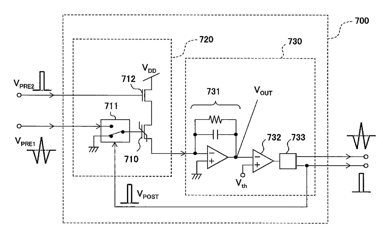
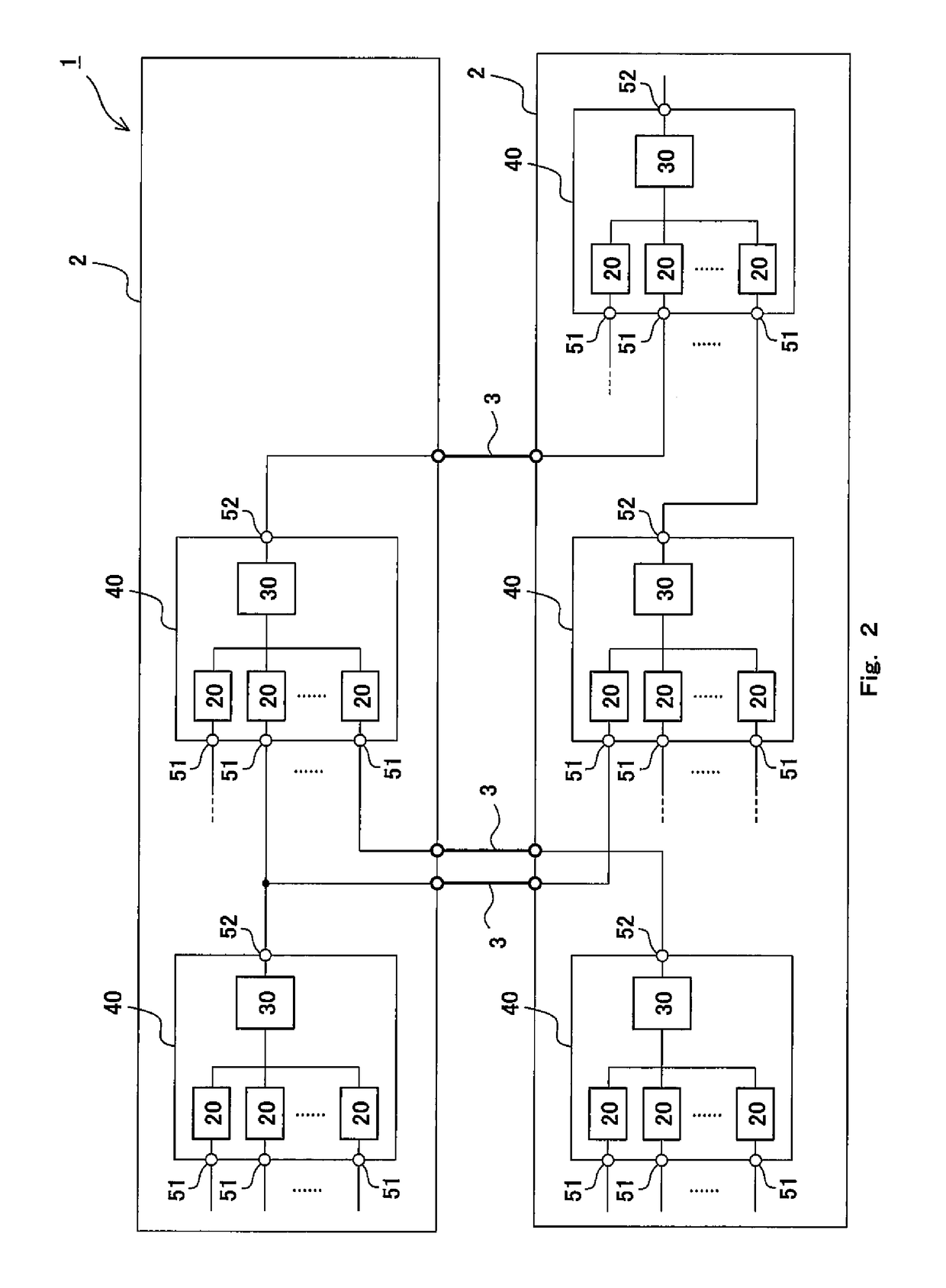
[0091]First of all, Embodiment 1 of the present disclosure will be described. FIG. 1 is a block diagram showing the schematic configuration of a neural network circuit element 40 included in a neural network circuit according to Embodiment 1 of the present disclosure. FIG. 2 is a block diagram showing the exemplary configuration of the neural network circuit 1 incorporating the neural network circuit element 40 of FIG. 1. As shown in FIG. 1, the neural network circuit element 40 of the present embodiment includes at least one input terminal 51, a synapse circuit 20 which is equal in number to the input terminal 51, one neuron circuit 30, and one output terminal 52. As shown in FIG. 2, the neural network circuit 1 is configured to include a plurality of neural network circuit elements 40 which are interconnected. Specifically, the output terminal 52 of the neural network circuit element 40 is connected to the input terminal 51 of another neural network circuit element 40.

[0092]The in...

embodiment 2

[0155]Next, Embodiment 2 of the present disclosure will be described. FIG. 15A is a cross-sectional view showing the schematic configuration of a floating gate transistor 80 used as the variable resistance element 10 in the synapse circuit according to Embodiment 2 of the present disclosure. FIG. 15B is a view showing the circuit symbol of the floating gate transistor 80 of FIG. 15A. In the present embodiment, the overall configuration of the neural network circuit is similar to that of FIGS. 1 and 2. The neural network circuit of the present embodiment is different from the neural network circuit of Embodiment 1 in that the floating gate transistor 80 is used as the variable resistance element 10.

[0156]As shown in FIG. 15A, the floating gate transistor 80 includes a semiconductor layer 82 provided on a substrate 81, a first dielectric layer 83 provided on a portion of the semiconductor layer 82, a floating gate electrode 84 provided on the first dielectric layer 83, a second dielec...


PUM


Abstract

In a neural network circuit element, a neuron circuit includes a waveform generating circuit for generating an analog pulse voltage, and a switching pulse voltage which is input as a first input signal to another neural network circuit element; a synapse circuit is configured such that the analog pulse voltage generated in the neuron circuit of the neural network circuit element including the synapse circuit is input to a third terminal of a variable resistance element of the synapse circuit, for a permissible input period, in the first input signal from another neural network circuit element; and the synapse circuit is configured such that the resistance value of the variable resistance element is changed in response to an electric potential difference between a first terminal and the third terminal, which occurs depending on a magnitude of the analog pulse voltage for the permissible input period.

Description

CROSS REFERENCE TO RELATED APPLICATION[0001]This is a continuation application under 35 U.S.C. 111(a) of pending prior International Application No. PCT / JP2014 / 002570, filed on May 15, 2014, which in turn claims the benefit of Japanese Application No. 2013-140389, filed on Jul. 4, 2013, the disclosures of which Applications are incorporated by reference herein.BACKGROUND OF THE DISCLOSURE[0002]1. Field of the Invention[0003]The present disclosure relates to a neural network circuit, and a learning method thereof.[0004]2. Description of the Related Art[0005]At present, computers which simulate information processing method of brains of living bodies have been studied. The most basic processing model of this is a neural network. Japanese Laid-Open Patent Application Publication No. Hei. 7-114524 (patent literature 1) discloses a model (pulse density model) which represents information using pulse densities. Patent literature 1 discloses that the model using pulses has a higher computi...

Claims


Application Information

Patent Timeline
Patent Type & Authority Patents(United States)
IPC IPC(8): G06N3/04G06N3/063G06N3/08
CPCG06N3/04G06N3/08G06N3/063G06N3/049
Inventor NISHITANI, YUKANEKO, YUKIHIROUEDA, MICHIHITO
Owner PANASONIC INTELLECTUAL PROPERTY MANAGEMENT CO LTD
Why Eureka
Try Eureka