Methods and systems relating to optical waveguide tapers

a technology of optical waveguides and taper rings, applied in the field of optical waveguide taper rings, to achieve the effect of reducing loss and constant loss per taper

Active Publication Date: 2017-11-28
MCGILL UNIV
View PDF5 Cites 5 Cited by
  • Summary
  • Abstract
  • Description
  • Claims
  • Application Information

AI Technical Summary

Benefits of technology

[0009]It is an object of the present invention to mitigate limitations in the prior art relating to optical waveguide tapers and more particularly to a new class of optical waveguide tapers that exhibit constant loss per taper segment with reduced loss to prior art tapers.

Problems solved by technology

However, these tend to be high loss and absorb valuable die footprint such that it would be beneficial to provide SOI PIC designers with a taper geometry that offers lower insertion loss and smaller footprint than the prior art but maintains compatibility with standard manufacturing methodologies.

Method used


Image

  • Methods and systems relating to optical waveguide tapers
  • Methods and systems relating to optical waveguide tapers
  • Methods and systems relating to optical waveguide tapers

Examples


Embodiment Construction

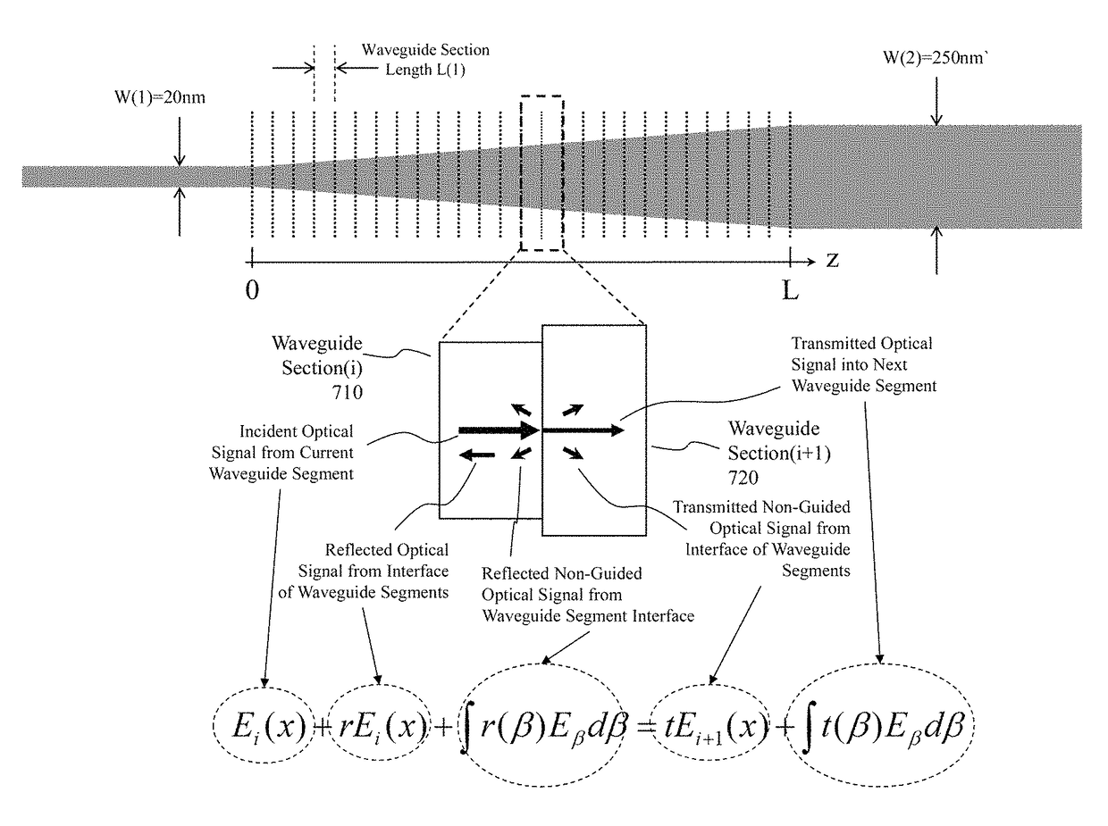
[0040]The present invention is directed to optical waveguide tapers and more particularly to a new class of optical waveguide tapers that exhibit constant loss per taper segment with reduced loss to prior art tapers.

[0041]The ensuing description provides exemplary embodiment(s) only, and is not intended to limit the scope, applicability or configuration of the disclosure. Rather, the ensuing description of the exemplary embodiment(s) will provide those skilled in the art with an enabling description for implementing an exemplary embodiment. It being understood that various changes may be made in the function and arrangement of elements without departing from the spirit and scope as set forth in the appended claims.

[0042]A: Constant Loss Tapers

[0043]A1. Introduction

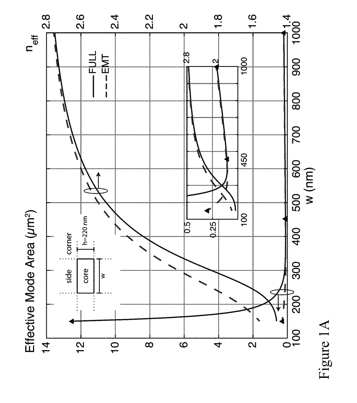
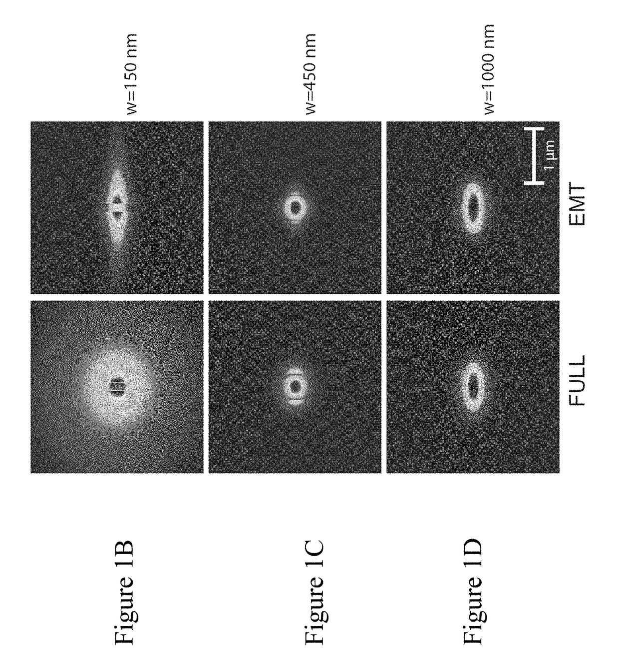
[0044]The large index of refraction contrast of a silicon-on-insulator (SOI) platform enables high density, cost-effective photonics on a chip. The typical interconnecting channel waveguide on 220 nm SOI has a 450 nm width...


PUM


Abstract

Photonic integrated circuits required connection to germanium doped silica cored optical fibers or silica cored and fluorine doped silica cladding optical fibers which have low index contrast and large mode field diameters. However, the optical waveguide within a photonic integrated circuit such as formed using silicon-on-insulator or compound semiconductors tends to be high index contrast and small mode field diameter. Accordingly, it is necessary to implement adiabatic waveguide tapers with a high coupling efficiency and small footprint in order to couple into the photonic integrated circuits to / from the optical fiber. Prior art tapers have been generally high loss and absorb valuable die footprint. In contrast the inventors demonstrate a small low loss waveguide taper designed using a methodology they refer to a “constant loss”.

Description

CROSS-REFERENCE TO RELATED APPLICATIONS[0001]This patent application claims the benefit of priority from U.S. Provisional Patent Application 62 / 163,498 filed May 19, 2015, currently pending, entitled “Methods and Systems Relating to Optical Waveguide Tapers”, the entire contents of which are incorporated herein by reference.FIELD OF THE INVENTION[0002]This invention relates to optical waveguide tapers and more particularly to a new class of optical waveguide tapers that exhibit constant loss per taper segment with reduced loss to prior art tapers.BACKGROUND OF THE INVENTION[0003]Silicon photonics exploiting silicon photonic integrated circuits (PICs) relates to the application of photonic systems which use silicon as an optical medium. The silicon is usually patterned with sub-micrometer precision, into photonic components and photonic integrated circuits which operate in the infrared, most commonly at the 1550 nm (1.55 μm) wavelength window used by most fiber optic telecommunicatio...

Claims


Application Information

Patent Timeline
Patent Type & Authority Patents(United States)
IPC IPC(8): G02B6/122G02B27/00G02B6/30G02B6/126
CPCG02B6/1228G02B27/0012G02B6/305G02B6/126
Inventor HORTH, ALEXANDREQUITORIANO, NATHANIEL
Owner MCGILL UNIV
Why Eureka
Try Eureka