

Near-unity photoluminescence quantum yield in MoS2
a photoluminescence and quantum yield technology, applied in the field of semiconductor emitters and detectors, can solve the problems of reduced surface recombination velocity after treatment, strong performance limit, and unstable hf treatmen
- Summary
- Abstract
- Description
- Claims
- Application Information
AI Technical Summary
Benefits of technology
Problems solved by technology
Method used
Image

Examples
Embodiment Construction
[0031]In the discussions that follow, various process steps may or may not be described using certain types of manufacturing equipment, along with certain process parameters. It is to be appreciated that other types of equipment can be used, with different process parameters employed, and that some of the steps may be performed in other manufacturing equipment without departing from the scope of this invention. Furthermore, different process parameters or manufacturing equipment could be substituted for those described herein without departing from the scope of the invention.
[0032]These and other details and advantages of the present invention will become more fully apparent from the following description taken in conjunction with the accompanying drawings.
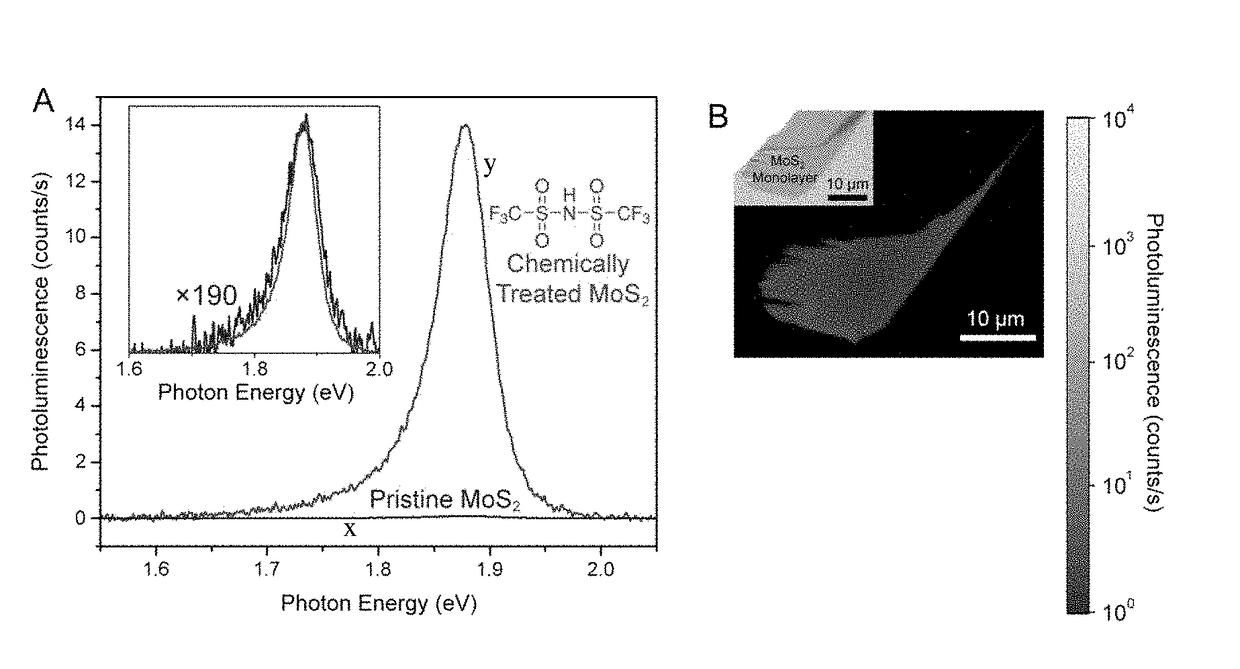
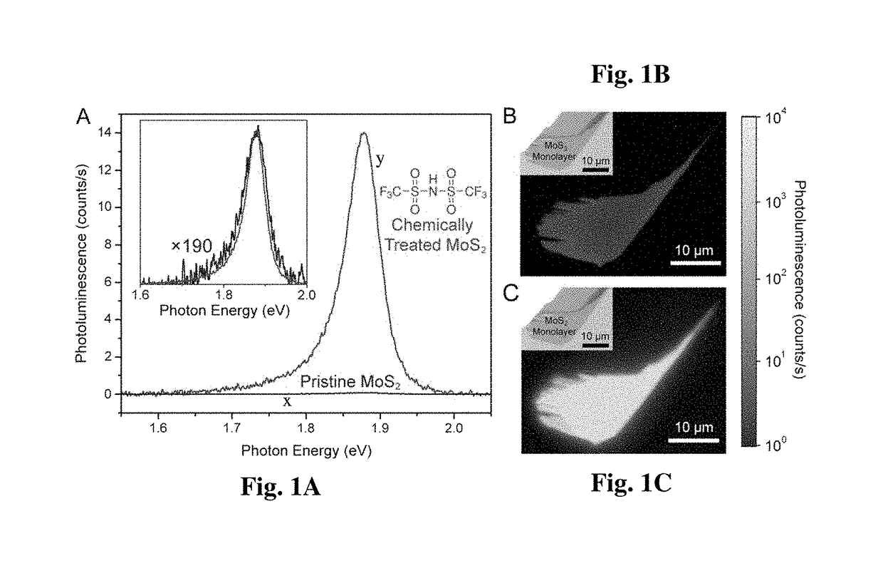
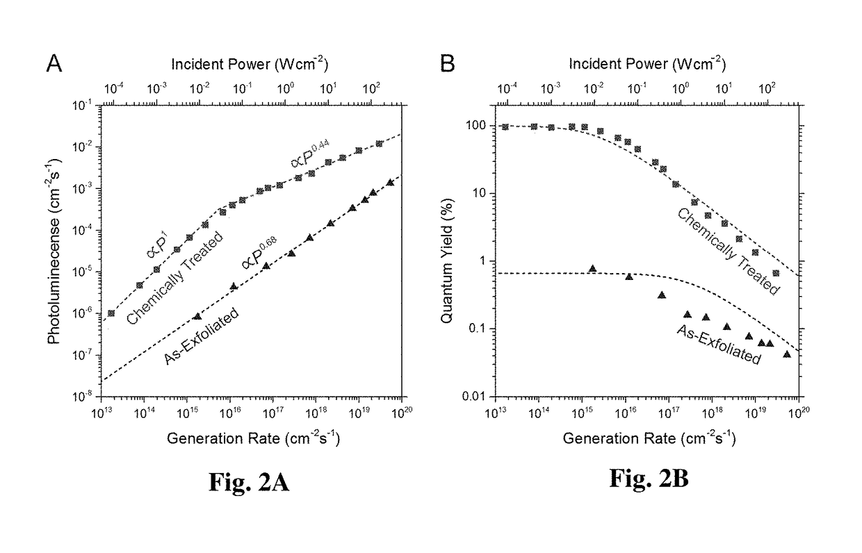
[0033]Monolayer transition metal dichalcogenide (TMDCs) have properties that make them highly suitable for optoelectronics, including the ability to form “van der Waals heterostructures” without the need for lattice matching, circ...
PUM
| Property | Measurement | Unit |
|---|---|---|
| temperature | aaaaa | aaaaa |
| photoluminescence quantum yield | aaaaa | aaaaa |
| binding energies | aaaaa | aaaaa |
Abstract
Description
Claims
Application Information