Communication system comprising a connector having first and second waveguides disposed in proximity to each other for coupling millimeter-wave data signals

a communication system and connector technology, applied in the direction of transmission, coupling device, electrical apparatus, etc., can solve the problems of radio wave leakage outside the chassis and degraded transmission characteristics, so as to suppress the degradation of transmission characteristics and suppress the leakage of radio wav

Active Publication Date: 2018-01-09
SONY SEMICON SOLUTIONS CORP
View PDF17 Cites 4 Cited by
  • Summary
  • Abstract
  • Description
  • Claims
  • Application Information

AI Technical Summary

Benefits of technology

[0010]The connector system, the communication device, or the communication system having the above-mentioned structure establishes communication when the opening terminal of one waveguide is in contact with or in the vicinity of the opening terminal of the other waveguide. Because of this, the connector system, the communication device, or the communication system is capable of suppressing more radio waves leaking externally than wireless communication using slot antennas. Moreover, the dielectric plate is provided on at least one of the opening terminal surfaces of the waveguides of the two communication devices. As a result, metal is not exposed on the contact surface.
[0011]According to the present disclosure, it is possible to suppress more radio waves leaking externally than wireless communication using slot antennas. As a result, it is possible to suppress degradation of transmission characteristics resulting from leakage of radio waves.
[0012]Note that effects are not necessarily limited to the above-mentioned effects. Any effect described in this specification may be obtained. Moreover, the effects described in this specification are only examples. Effects are not limited to the effects described in this specification. Moreover, additional effects may be obtained.

Problems solved by technology

Because of this, radio waves easily leak outside of the chassis.
As a result, transmission characteristics may be degraded.

Method used


Image

  • Communication system comprising a connector having first and second waveguides disposed in proximity to each other for coupling millimeter-wave data signals
  • Communication system comprising a connector having first and second waveguides disposed in proximity to each other for coupling millimeter-wave data signals
  • Communication system comprising a connector having first and second waveguides disposed in proximity to each other for coupling millimeter-wave data signals

Examples


example 1

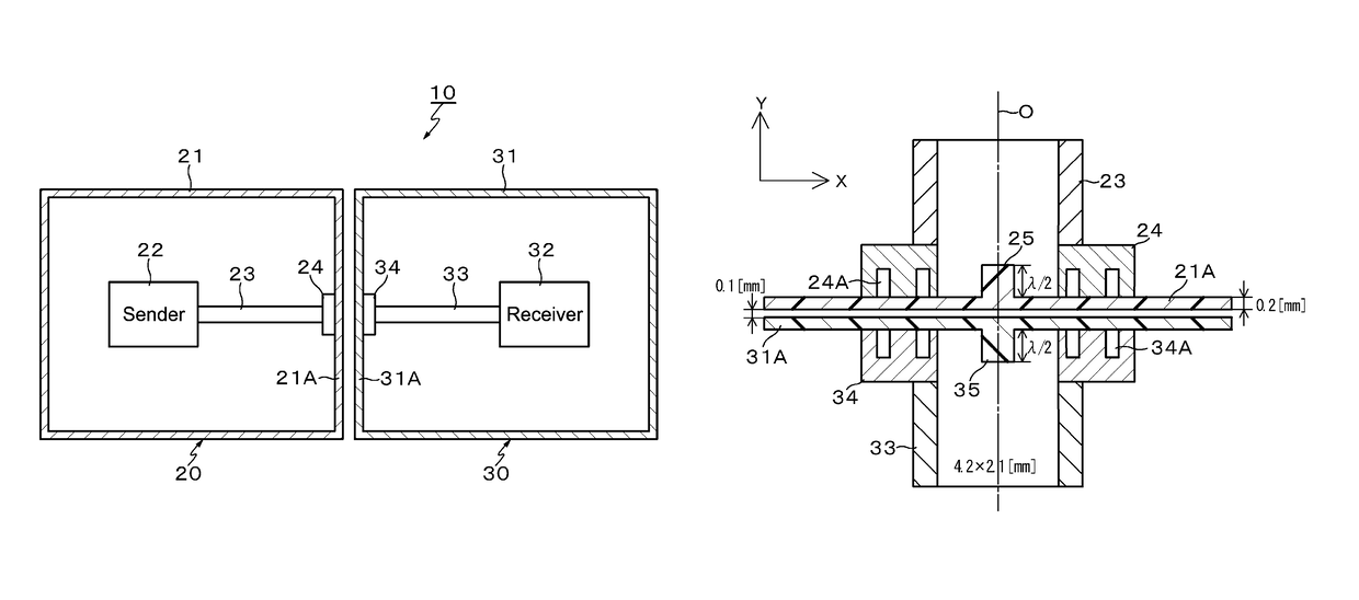
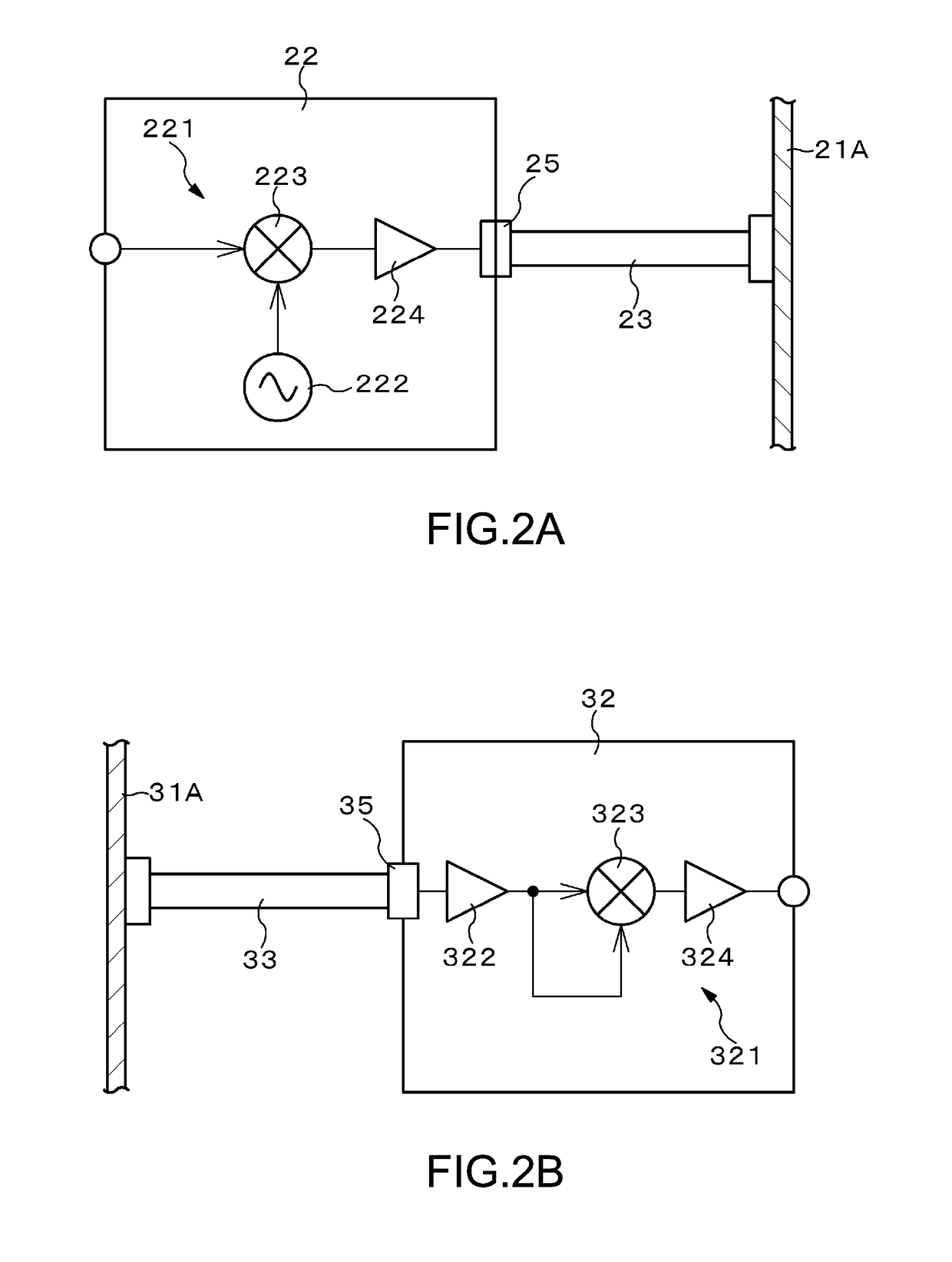
[0065]FIG. 6A is a side view partially including a sectional view showing the first communication device 20 and the second communication device 30 of Example 1. An IC chip, which is the sender 22 configured to send a millimeter-waveband signal, and other components are mounted on a board 26. An IC chip, which is the receiver 32 configured to receive a millimeter-waveband signal, and other components are mounted on a board 36. A track 27 such as a microstripline is provided between the output terminal of the sender 22 and one opening terminal of the waveguide 23. A track 37 such as a microstripline is provided between the input terminal of the receiver 32 and one opening terminal of the waveguide 33. The other opening terminal (i.e., the opening terminal at the choke structure 24 side) of the waveguide 23 is attached to the resin plate 21A. The other opening terminal (i.e., the opening terminal at the choke structure 34 side) of the waveguide 33 is attached to the resin plate 31A. Th...

example 2

[0066]FIG. 6B is a side view partially including a sectional view showing the first communication device 20 and the second communication device 30 of Example 2. Example 2 is characterized in that the IC chip (the sender 22) is mounted on the board 26, the surface of the board 26 opposite to the IC chip faces the resin plate 21A, and the waveguide 23 is mounted on the opposite surface. Example 2 is further characterized in that the IC chip (the receiver 32) is mounted on the board 36, the surface of the board 36 opposite to the IC chip faces the resin plate 31A, and the waveguide 33 is mounted on the opposite surface. In Example 2, the IC chip (the sender 22) connects with the waveguide 23 through a via hole 29, and the IC chip (the receiver 32) connects with the waveguide 33 through a via hole 39.

modification examples of examples

[0067]In the above-mentioned typical Examples 1 and 2, each of the first communication device 20 and the second communication device 30 is a module including a waveguide. This is merely an example. Alternatively, the following modification examples may be employed. As shown in FIG. 7 and FIG. 8, a connector device including the waveguide 23, the resin plate 21A, and the dielectric protrusion 25 (not shown in FIGS. 7 and 8) is independent of a module unit including the IC chip (the sender 22), the board 26, and the like, and the connector device connects with the module unit through a transmission path 41 such as a cable or a waveguide. A connector device including the waveguide 33, the resin plate 31A, and the dielectric protrusion 35 (not shown in FIGS. 7 and 8) is independent of a module unit including the IC chip (the receiver 32), the board 36, and the like, and the connector device connects with the module unit through a transmission path 42 such as a cable or a waveguide. Acco...


PUM


Abstract

Provided is a connector system including a first waveguide having a first opening terminal and a second waveguide having a second opening terminal. The first and second waveguides transmit a high-frequency signal when the first opening terminal is in contact with or in the vicinity of the second opening terminal. A dielectric plate is provided on an opening terminal surface of at least one of the first and second opening terminals.

Description

CROSS REFERENCE TO RELATED APPLICATIONS[0001]This application claims the benefit of Japanese Priority Patent Application JP 2014-054564 filed Mar. 18, 2014, the entire contents of which are incorporated herein by reference.BACKGROUND[0002]The present disclosure relates to a connector system, a communication device, and a communication system.[0003]There is known such a following communication system. One communication device communicates with the other communication device when one chassis (device body) is in contact with or in the vicinity of the other chassis (device body). As an example of this kind of communication system, there is known a communication system including two communication devices, i.e., a mobile terminal device and a wireless communication device called a cradle (for example, see Japanese Patent Application Laid-open No. 2006-65700).SUMMARY OF THE INVENTION[0004]In this communication system, one communication device communicates with the other communication devic...

Claims


Application Information

Patent Timeline
Patent Type & Authority Patents(United States)
IPC IPC(8): H04B3/52H04B1/40H04B5/00H01P1/04H01P5/02H01P1/08
CPCH04B3/52H01P1/042H04B1/40H04B5/0031H01P5/024H01P1/08
Inventor OKADA, YASUHIRO
Owner SONY SEMICON SOLUTIONS CORP
Why Eureka
Try Eureka