In line critical path delay measurement for accurate timing indication for a first fail mechanism

a critical path and delay measurement technology, applied in the field of ultralow power integrated circuits, can solve the problems of not being able to help mimic the delay and not being able to allow separate measurement, and achieve the effect of optimal device power consumption and safe use of functional circuitry

a critical path and delay measurement technology, applied in the field of ultralow power integrated circuits, can solve the problems of not being able to help mimic the delay and not being able to allow separate measurement, and achieve the effect of optimal device power consumption and safe use of functional circuitry

US9882564B1Active Publication Date: 2018-01-30NXP ISRAEL LTD

Image

  • In line critical path delay measurement for accurate timing indication for a first fail mechanism
  • In line critical path delay measurement for accurate timing indication for a first fail mechanism
  • In line critical path delay measurement for accurate timing indication for a first fail mechanism

Examples


Embodiment Construction

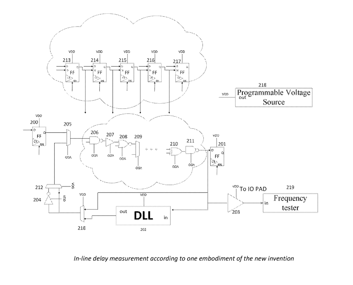
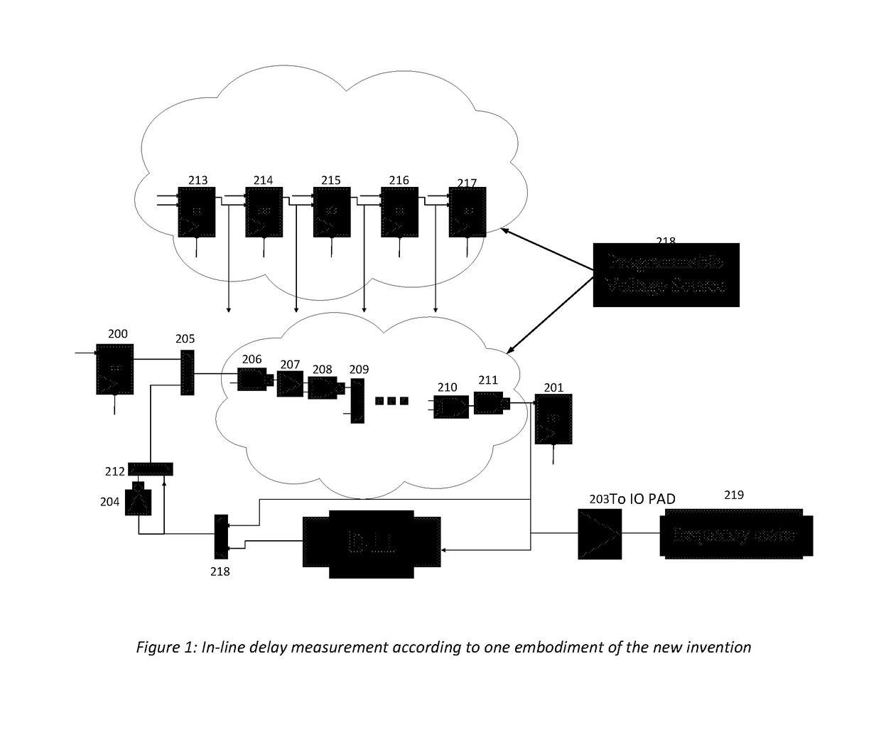
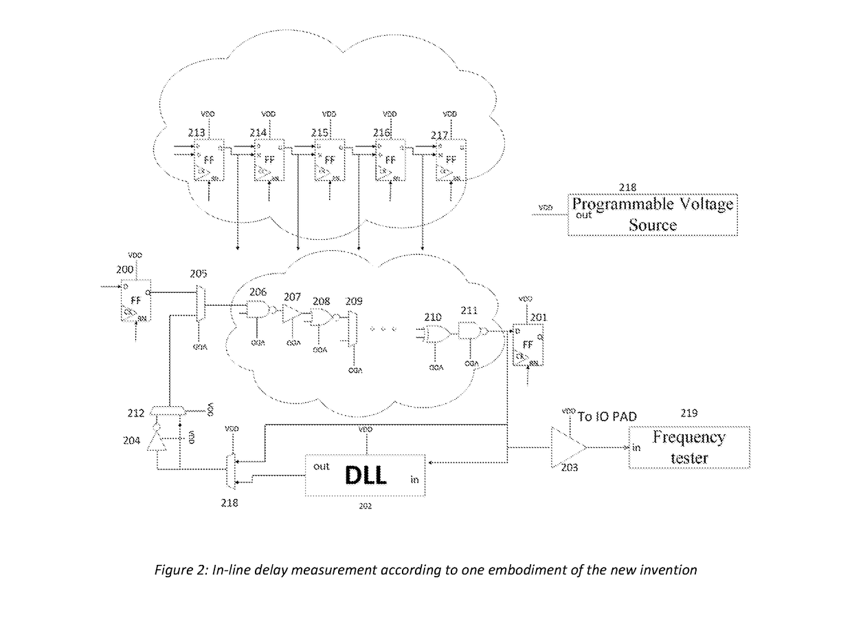
[0025]The present invention includes a method and apparatus for accurate in-line measurement of a device critical path timing (critical path is the longest electrical path passing plurality of combinational cells between two flops of the device, that is to say having the time to the longest transmission) in order to mimic this delay into a separate programmable DLL First Fail circuit, which will be used in order to dynamically control the operating voltage of the device to get optimal power consumption.

[0026]In the following description, numerous specific details are set forth. However, it is understood that embodiments of the invention may be practiced without these specific details. In other instances, well-known circuits, structures and techniques have not been shown in detail in order not to obscure the understanding of this description.

[0027]Reference throughout the specification to “one embodiment” or “an embodiment” means that a particular feature, structure, or characteristi...


PUM


Abstract

A method for implementing a programmable critical delay path measurement in-line with the critical path logic cells. Additionally, the delay measurement creates a code to be used with a programmable DLL which indicates the delay of the measured critical path. This code can also be used by an off line First Fail Circuit which can mimic the delay of the critical path and give an indication of the critical path delay. The target of this invention is to create a method to optimize the required operating voltage of an integrated circuit per specific speed requirement, overcoming different process variations, temperatures changes and in die variations.

Description

FIELD OF THE INVENTION[0001]The invention relates to the development of ultra-low power integrated circuits and, more specifically, to the characterization of the critical path timing using a programmable DLL and a way to mimic this delay using a first Fail Circuit.BACKGROUND OF THE INVENTION[0002]Many new emerging applications require the use of ultra-low power consumption solutions inside a chip. This will allow them to be incorporated into devices that operate from a small non-chargeable battery for very long periods without the need to frequently charge the battery. For example, wearable, mobile and Medical devices which are battery operated may require an ultra-low power solution.[0003]In parallel the scaling of the silicon manufacturing geometry doubles every 2 years creating larger and faster chips which include many more transistors and logic inside that are running at higher speed and consume more power. In addition to this, the advanced process become less controllable and...

Claims


Application Information

Patent Timeline
30 Jan 2018
Publication
US9882564B1
IPC
H03K5/13; H03K19/00; H03K5/159; G01R31/3183; H03K19/003; G01R31/3177; G01R31/3185; H03K5/135; H03K5/156
CPC
H03K5/156; H03K19/00323; H03K19/0008; H03K5/159; G01R31/318328; G01R31/31858; H03K5/135; G01R31/3177
Inventors
ZANGI, UZI; FELDMAN, NEIL