Electronic package and fabrication method thereof

a technology of electronic packaging and fabrication method, which is applied in the direction of electrical equipment, semiconductor devices, semiconductor/solid-state device details, etc., can solve the problems of adversely affecting the process yield and increasing the fabrication cost, residue may adversely affect the electrical transmission performance of the conductive posts, and the conductive post cannot meet the fine pitch requirement, so as to improve the electrical transmission performance of the first conductor, improve the process yield, and easy to remove residue

Active Publication Date: 2018-02-20
SILICONWARE PRECISION IND CO LTD
View PDF6 Cites 2 Cited by
  • Summary
  • Abstract
  • Description
  • Claims
  • Application Information

AI Technical Summary

Benefits of technology

[0027]Further, since the aspect ratio of the first via hole does not increase, the first via hole can be effectively and completely plated with the first conductor.
[0028]Furthermore, since both the first via hole and the second via hole are less in depth than the through hole, the present invention can easily remove residue in the first via hole and the second via hole so as to improve the electrical transmission performance of the first conductor and the second conductor. Therefore, the present invention improves the process yield and reduces the fabrication cost.

Problems solved by technology

As such, the electronic package 1 cannot meet the fine pitch requirement.
On the other hand, if the aspect ratio in laser drilling is increased to 1.5, the bottom of the through hole 110′ cannot be completely filled with copper through the electroplating process (i.e., an unplated area 12′ is formed), as shown in FIG. 1E′, thus adversely affecting the process yield and increasing the fabrication cost.
Otherwise, the residue may adversely affect the electrical transmission performance of the conductive posts 110.
However, if the thickness of the insulating layer 11 is increased, i.e., the depth H of the through holes 110 is increased, it will become difficult to completely remove the residue in the through holes 110.
As such, the electrical transmission performance of the conductive posts 110 may be adversely affected by the remaining residue.

Method used


Image

  • Electronic package and fabrication method thereof
  • Electronic package and fabrication method thereof
  • Electronic package and fabrication method thereof

Examples


Embodiment Construction

[0031]The following illustrative embodiments are provided to illustrate the disclosure of the present invention, these and other advantages and effects can be apparent to those in the art after reading this specification.

[0032]It should be noted that all the drawings are not intended to limit the present invention. Various modifications and variations can be made without departing from the spirit of the present invention. Further, terms such as “first”, “second”, “on”, “a” etc. are merely for illustrative purposes and should not be construed to limit the scope of the present invention.

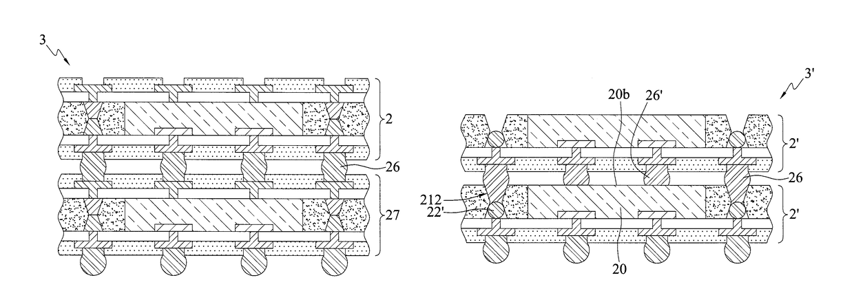
[0033]FIGS. 2A to 2G are schematic cross-sectional views showing a method for fabricating an electronic package 2, 2′, 3, 3′ according to the present invention.

[0034]Referring to FIG. 2A, a carrier (not shown) having at least an electronic element 20 disposed thereon is provided and an insulating layer 21 is formed on the carrier to encapsulate the electronic element20. Then, the carrier is removed.

[00...


PUM


Abstract

A method for fabricating an electronic package is provided, which includes the steps of: providing an insulating layer having at least an electronic element embedded therein; forming at least a first via hole on one side of the insulating layer; forming a first conductor in the first via hole of the insulating layer; forming on the insulating layer a first circuit structure electrically connected to the electronic element and the first conductor; and forming a second via hole on the other side of the insulating layer, wherein the second via hole communicates with the first via hole. As such, the second via hole and the first via hole constitute a through hole. Since the through hole is fabricated through two steps, the aspect ratio (depth / width) of the through hole can be adjusted according to the practical need so as to improve the process yield.

Description

CROSS-REFERENCES TO RELATED APPLICATIONS[0001]This application claims under 35 U.S.C. § 119(a) the benefit of Taiwanese Application No. 103135624, filed Oct. 15, 2014 the entire contents of which are incorporated herein by reference.BACKGROUND OF THE INVENTION[0002]1. Field of the Invention[0003]The present invention relates to packaging processes, and more particularly, to an electronic package and a fabrication method thereof so as to improve the process yield.[0004]2. Description of Related Art[0005]Through molding via (TMV) technology has been widely applied in semiconductor fields, which mainly involves forming via holes on a surface of an encapsulant by laser drilling so as to increase routing space. For example, a fan-out package on package (PoP) structure can be achieved by using TMV technology.[0006]FIGS. 1A to 1F are schematic cross-sectional views showing a method for fabricating an electronic package 1 of a fan-out PoP structure according to the prior art.[0007]Referring...

Claims


Application Information

Patent Timeline
Patent Type & Authority Patents(United States)
IPC IPC(8): H01L23/49H01L23/00H01L23/498H01L23/538H01L25/10H01L25/00H01L21/48H01L21/56
CPCH01L23/49811H01L24/19H01L24/20H01L25/105H01L25/50H01L23/5389H01L2924/18162H01L21/486H01L21/568H01L24/96H01L2224/04105H01L2224/12105H01L2225/1035H01L2225/1041H01L2225/1058
Inventor CHEN, YAN-HENGLIN, CHUN-TANGCHAN, MU-HSUANCHI, CHIEH-YUAN
Owner SILICONWARE PRECISION IND CO LTD
Why Eureka
Try Eureka