Multilayer ceramic electronic component and method for manufacturing multilayer ceramic electronic component

a technology of electronic components and ceramics, applied in the direction of fixed capacitors, stacked capacitors, fixed capacitor details, etc., can solve the problems of difficult to adjust the degree of oxidation and expansion, and difficult to ensure electrical connection between the inner electrode and the outer electrode, so as to reduce the occurrence of electrical discharge troubles and increase the amount of electric discharge. , the effect of preventing the occurrence of electric discharg

Active Publication Date: 2018-02-27
MURATA MFG CO LTD
View PDF17 Cites 1 Cited by
  • Summary
  • Abstract
  • Description
  • Claims
  • Application Information

AI Technical Summary

Benefits of technology

[0009]In the light of the above circumstances, preferred embodiments of the present invention provide a multilayer ceramic electronic component in which, even when laminated inner electrode layers and / or ceramic layers are thin films, the inner electrode layers and an outer electrode are electrically connected to each other with reliability, and a method for manufacturing the multilayer ceramic electronic component.
[0011]In the above-described configuration, in accordance with the thin portion whose thickness in the vicinity of the first end portion continuously reduces toward the first end portion included in each of the ceramic layers, each of the inner electrode layers includes the thick portion in the vicinity of the connection with the outer electrode, the thick portion having the thickness continuously increasing toward the connection on the first side. Accordingly, because the area of the connection between the outer electrode and the inner electrode layers is large, even when the inner electrode layers are thin films, the inner electrode layers and the outer electrode are electrically connected to each other with reliability. If a thick portion is simply provided in each of the inner electrode layer in the vicinity of the connection with the outer electrode, the distance between a second end portion that is not joined to the outer electrode and the thick portion in the inner electrode layer adjacent thereto may be equal to or shorter than the interlayer distance between the inner electrode layers, as indicated in a drawing illustrated below. In that case, an electric field may concentrate in the second end portion in the inner electrode and the amount of electric discharge may increase. In contrast, in the above-described configuration, because the distance between the second end portion, which is not joined to the outer electrode, and the thick portion in the adjacent inner electrode layer is equal to or longer than the interlayer distance between the inner electrode layers, the occurrence of concentration of an electric field in the second end portion in the inner electrode layer is significantly reduced, and the possibility of increasing the amount of electric discharge is prevented. Accordingly, a highly reliable multilayer ceramic electronic component in which the occurrence of troubles caused by electric discharge is significantly is provided.
[0016]In the above-described configuration, the highly reliable multilayer ceramic electronic component in which the occurrence of troubles caused by electric discharge is significantly reduced is thus manufactured.
[0018]In the above-described configuration, the use of the united portions in the inner electrode layers as the outer electrode eliminates a step of newly forming the outer electrode.
[0021]According to the above-described configuration, by forming the ceramic layer such that it includes the thin portion whose thickness in the vicinity of the first end portion continuously reduces toward the first end portion, the inner electrode layer is formed such that it includes the thick portion in the vicinity of the connection with the outer electrode, the thick portion having the thickness that continuously increases toward the connection on the first side in accordance with the shape of the thin portion in the ceramic layer. Accordingly, because the area of the connection between the outer electrode and the inner electrode layers is large, even when the inner electrode layers are formed as thin films, the inner electrode layers and the outer electrode are electrically connected to each other with reliability. In addition, because the distance between the second end portion in each of the inner electrode layers, the second end portion being not joined to the outer electrode, and the thick portion in the inner electrode layer adjacent thereto is equal to or longer than the interlayer distance between the inner electrode layers, the occurrence of concentration of an electric field in the second end portion in the inner electrode layer is reduced, and the possibility of increasing the amount of electric discharge is prevented. Accordingly, a highly reliable multilayer ceramic electronic component in which the occurrence of troubles caused by electric discharge is significantly reduced is provided.

Problems solved by technology

However, it is difficult to adjust the degree of oxidation and expansion.
In particular, when the inner electrodes are thin, they become separated more easily from the end surfaces of the ceramic sinter, and a problem arises in that it is difficult to ensure electrical connection with the outer electrodes.
In such a case, it is impossible to ensure electrical connection between the inner electrodes and the outer electrodes.

Method used


Image

  • Multilayer ceramic electronic component and method for manufacturing multilayer ceramic electronic component
  • Multilayer ceramic electronic component and method for manufacturing multilayer ceramic electronic component
  • Multilayer ceramic electronic component and method for manufacturing multilayer ceramic electronic component

Examples


first preferred embodiment

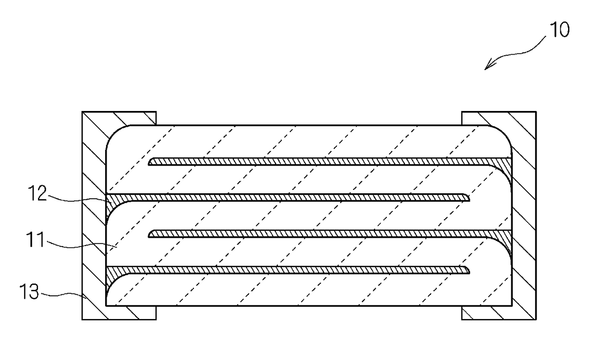
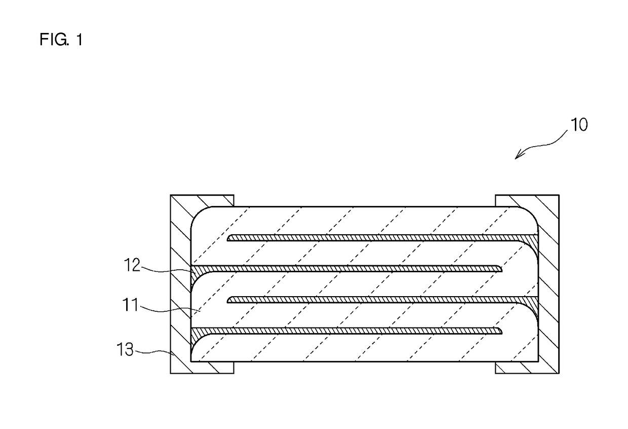
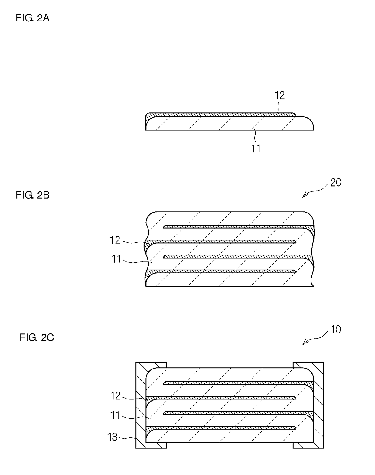
[0031]FIG. 1 is a cross-sectional view that illustrates a configuration of a multilayer ceramic electronic component according to a first preferred embodiment of the present invention. As illustrated in FIG. 1, ceramic layers 11 and inner electrode layers 12 are alternately laminated in a multilayer ceramic electronic component 10 according to the present first preferred embodiment, and an outer electrode 13 is disposed on both side surfaces thereof. The multilayer ceramic electronic component 10 according to the present first preferred embodiment has a characteristic in that each of the ceramic layer 11 includes a thin portion whose thickness continuously reduces in the vicinity of a first end portion. FIGS. 2A-2C are diagrams that schematically illustrate a method for manufacturing the multilayer ceramic electronic component 10 according to the first preferred embodiment of the present invention.

[0032]As illustrated in FIG. 2A, first, the ceramic layer 11 is formed such that it in...

second preferred embodiment

[0047]A multilayer ceramic electronic component according to a second preferred embodiment of the present invention has a characteristic in that the ceramic layers 11 and the inner electrode layers 12 are formed by an inkjet technique. FIGS. 6A-6D are diagrams for describing a method for manufacturing the multilayer body 20 in the multilayer ceramic electronic component 10 according to the second preferred embodiment of the present invention. The same reference numerals are used in the elements similar to those in the first preferred embodiment, and the detailed description thereof is omitted.

[0048]As illustrated in FIGS. 6A-6D, the multilayer body 20 in the multilayer ceramic electronic component 10 according to the present second preferred embodiment is produced by alternately laminating the ceramic layers 11 and the inner electrode layers 12. First, as illustrated in FIG. 6A, ceramic ink 62 is discharged and applied on a substrate (base) 60 while an ink head 61 is moved in a firs...


PUM

PropertyMeasurementUnit
thicknessaaaaaaaaaa
distanceaaaaaaaaaa
thickaaaaaaaaaa

Abstract

A multilayer ceramic electronic component includes a multilayer body including ceramic layers and inner electrode layers, the inner electrode layers being disposed on interfaces between the ceramic layers, and an outer electrode on an external surface of the multilayer body and electrically connected to first end portions of the inner electrode layers exposed to the external surface of the multilayer body. Each of the ceramic layers includes a thin portion with a continuously reducing thickness near the first end portion. Each inner electrode layer includes a thick portion near a connection with the outer electrode, the thick portion having a thickness continuously increasing toward the connection on a first side in accordance with a shape of the thin portion in the ceramic layer. A distance between a second end portion in the inner electrode layer not joined to the outer electrode, and the thick portion adjacent to the second end portion is equal to or longer than an interlayer distance between the inner electrode layers.

Description

BACKGROUND OF THE INVENTION[0001]1. Field of the Invention[0002]The present invention relates to a multilayer ceramic electronic component, such as a multilayer ceramic capacitor, and a method for manufacturing the multilayer ceramic electronic component. In particular, the present invention relates to a multilayer ceramic electronic component in which, even when laminated inner electrode layers and / or ceramic layers are thin films, the inner electrode layers are electrically connected to an outer electrode with reliability, and also the present invention relates to a method for manufacturing the multilayer ceramic electronic component.[0003]2. Description of the Related Art[0004]In recent years, further reduction in the size and the height profile of a multilayer ceramic electronic component, such as a multilayer ceramic capacitor, has been required. Thus, it is necessary to further reduce the thickness of an inner electrode, the thickness of a ceramic layer between the inner elect...

Claims


Application Information

Patent Timeline
Patent Type & Authority Patents(United States)
IPC IPC(8): H01G4/005H01G4/012H01G4/232H01G4/30H01G4/008H01G4/12
CPCH01G4/306H01G4/0085H01G4/232H01G4/30H01G4/012H01G4/12
Inventor HIRAO, TAKAHIRO
Owner MURATA MFG CO LTD
Why Eureka
Try Eureka