Silicon-on-insulator (SOI) structures with step-type buried oxide layers

A technology of buried oxide layer and oxide layer, applied in electrical components, semiconductor/solid-state device manufacturing, circuits, etc., can solve problems such as increased leakage current, short channel effect, short channel, etc., to reduce leakage current and suppress Threshold voltage reduction and performance improvement effect

Active Publication Date: 2015-03-18
SHANGHAI HUAHONG GRACE SEMICON MFG CORP
View PDF2 Cites 0 Cited by
  • Summary
  • Abstract
  • Description
  • Claims
  • Application Information

AI Technical Summary

Problems solved by technology

[0004] However, as the size of this SOI structure with a stepped buried oxide layer is miniaturized, specifically, the channel length becomes shorter, severe short channel effects will occur.
The short channel effect is specifically manifested as: (1) the threshold voltage decreases continuously as the channel length becomes shorter; (2) as the channel length becomes shorter, the depletion layer of the drain region and the source region are very close, in When the source region and the drain region are biased, the electric field lines in the channel can cross from the drain region to the source region, and cause the barrier height of the source region to decrease, resulting in the SOI structure being in the off state, that is, V GS When the turn-on voltage is not reached, the leakage current increases, which is not conducive to the performance of SOI structure devices
[0005] In view of this, it is necessary to propose a new SOI structure with a stepped buried oxide layer to solve the short channel effect of the existing SOI structure.

Method used


Image

  • Silicon-on-insulator (SOI) structures with step-type buried oxide layers
  • Silicon-on-insulator (SOI) structures with step-type buried oxide layers
  • Silicon-on-insulator (SOI) structures with step-type buried oxide layers

Examples


no. 1 example

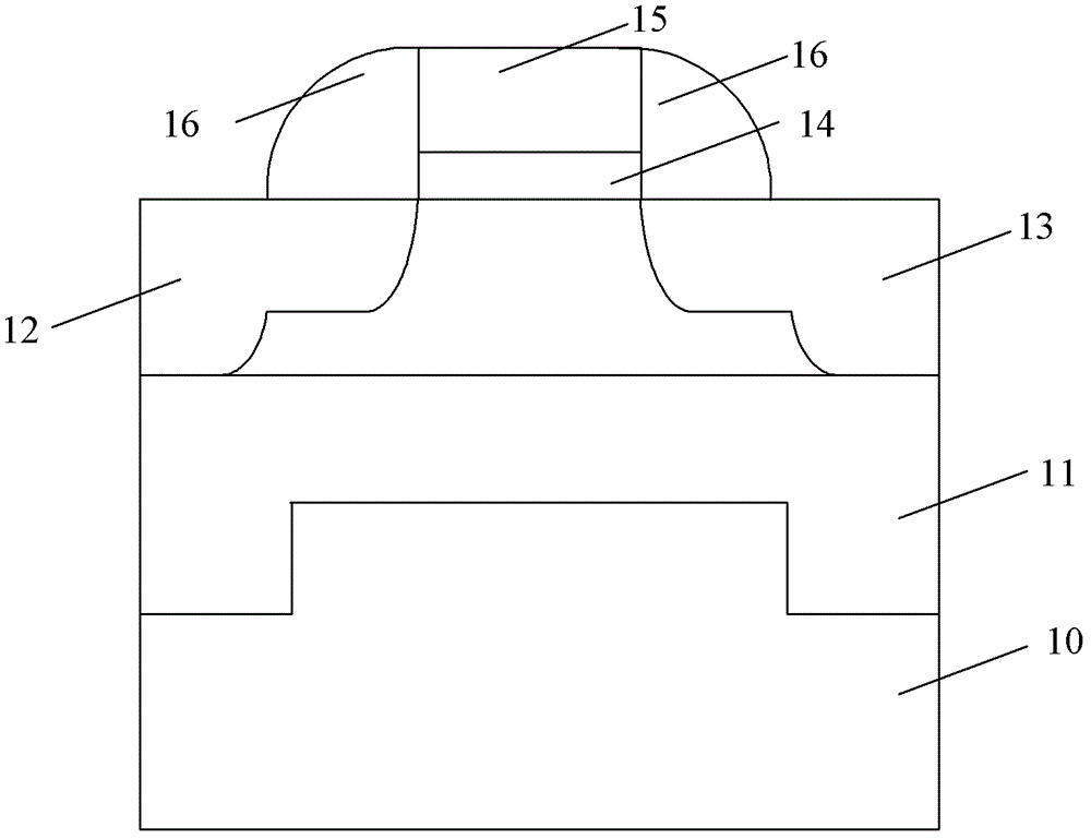
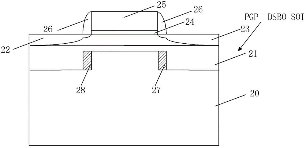
[0046] The SOI structure provided by this embodiment one is PGP DSBO SOI (Partially Ground Plane Double Step Buried Oxide SOI), such as image 3 shown, including:

[0047] P-type semiconductor substrate 20, on which an N-type source region 22, an N-type drain region 23, and a stepped oxide layer under the N-type source region 22, N-type drain region 23 and the P-type channel are formed 21; wherein, the thickness of the oxide layer 21 located in the N-type source region 22 and the N-type drain region 23 is respectively greater than the thickness of the oxide layer 21 located under the P-type channel;

[0048] a gate insulating layer 24 formed on the P-type channel;

[0049] a gate 25 on the gate insulating layer;

[0050] Covering the gate 25 and the sidewall 26 on the side of the gate insulating layer 24;

[0051] Wherein, a P-type element heavily doped region 27 is provided in the P-type semiconductor substrate 20 under the corresponding thinner oxide layer 21 under the si...

no. 2 example

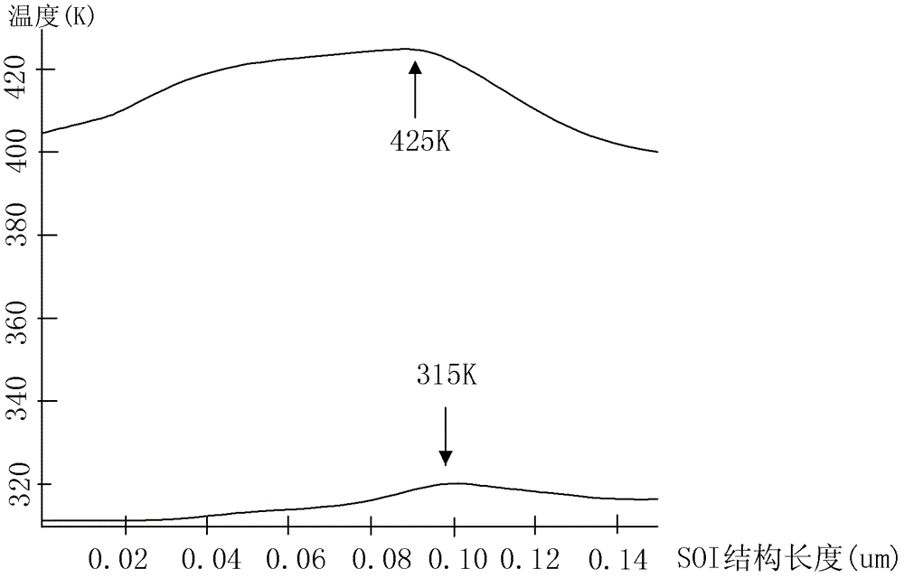
[0081] If the SOI structure provided by the first embodiment is called NMOS, the difference from the first embodiment is that the SOI structure provided by the second embodiment is PMOS. It can be understood that, regardless of NMOS or PMOS, the P-type element heavily doped region They are all regions with the lowest potential. Therefore, setting a P-type element heavily doped region in the PMOS SOI structure can also prevent the electric field lines drawn from the drain region in the existing DSBO SOI structure from partially terminating in the source region, and thus As a result, the barrier height at the end of the source region is reduced, which in turn causes electrons in the source region to easily cross the barrier and enter the drain region, which increases the threshold voltage of the SOI structure, reduces the leakage current when the SOI structure is in the off state, and improves the efficiency of the SOI structure. Performance of SOI structure devices.

[0082] Sp...


PUM


Abstract

The invention provides two types of silicon-on-insulator (SOI) structures with step-type buried oxide layers. The first type of SOI structure comprises a P-type semiconductor substrate, a gate insulation layer formed above a P-type channel, a grid electrode formed above the gate insulation layer and a side wall which covers the grid electrode and the side edge of the gate insulation layer, wherein an N-type source region, an N-type drain region, the step-type buried oxide layers positioned in the N-type source region and the N-type drain region and below the P-type channel are formed on the semiconductor substrate; the thicknesses of the buried oxide layers positioned in the N-type source region and the N-type drain region are respectively greater than that of the buried oxide layer positioned below the P-type channel; and a P-type element heavily doped region is arranged in the P-type semiconductor substrate below the corresponding thinner buried oxide layer below the side wall adjacent to one side of the N-type drain region. Different from the first type of SOI structure, the second type of SOI structure is characterized in that the top of the substrate is provided with the N-type doped region, and the source region and the drain region are P-type. By utilizing the technical scheme of the invention, the short channel effect of the existing SOI structures can be solved.

Description

technical field [0001] The invention relates to the field of semiconductor manufacturing, in particular to an SOI structure with a stepped oxide buried layer. Background technique [0002] In SOI (silicon-on-insulator) materials, because there is an insulating buried layer (usually a silicon dioxide buried layer, referred to as a buried oxide layer) between the top silicon film and the substrate silicon, SOI technology has many advantages beyond traditional bulk silicon. Technical advantages, such as: Compared with traditional bulk silicon CMOS, CMOS manufactured using SOI materials has the characteristics of high speed, low power consumption, and small source-drain parasitic capacitance, while avoiding the latch-up effect in bulk silicon CMOS. [0003] figure 1 Shown is an SOI structure with a buried oxide layer in the prior art, which includes: a semiconductor substrate 10, a gate insulating layer 14 and a gate 15 formed on the substrate 10, the gate insulating layer 14 a...

Claims


Application Information

Patent Timeline
Patent Type & Authority Patents(China)
IPC IPC(8): H01L21/762H01L29/06
Inventor 苟鸿雁
Owner SHANGHAI HUAHONG GRACE SEMICON MFG CORP
Why Eureka
Try Eureka