
Ultrasonic Diagnosis Device and Electronic Circuit

a diagnostic device and ultrasonic technology, applied in the field of ultrasonic diagnosis devices and electronic circuits, can solve the problems of degrading the s/n ratio and achieve the effects of reducing the noise of a plurality of memory cell arrays, and increasing the number of memory cells

Inactive Publication Date: 2020-01-23
FUJIFILM HEALTHCARE CORP
View PDF3 Cites 1 Cited by
  • Summary
  • Abstract
  • Description
  • Claims
  • Application Information

AI Technical Summary

Benefits of technology

The present invention aims to reduce or eliminate noise caused by multiple memory cell arrays. The technical effects of the invention include reducing noise without increasing the number of memory cells and minimizing the impact on performance.

Problems solved by technology

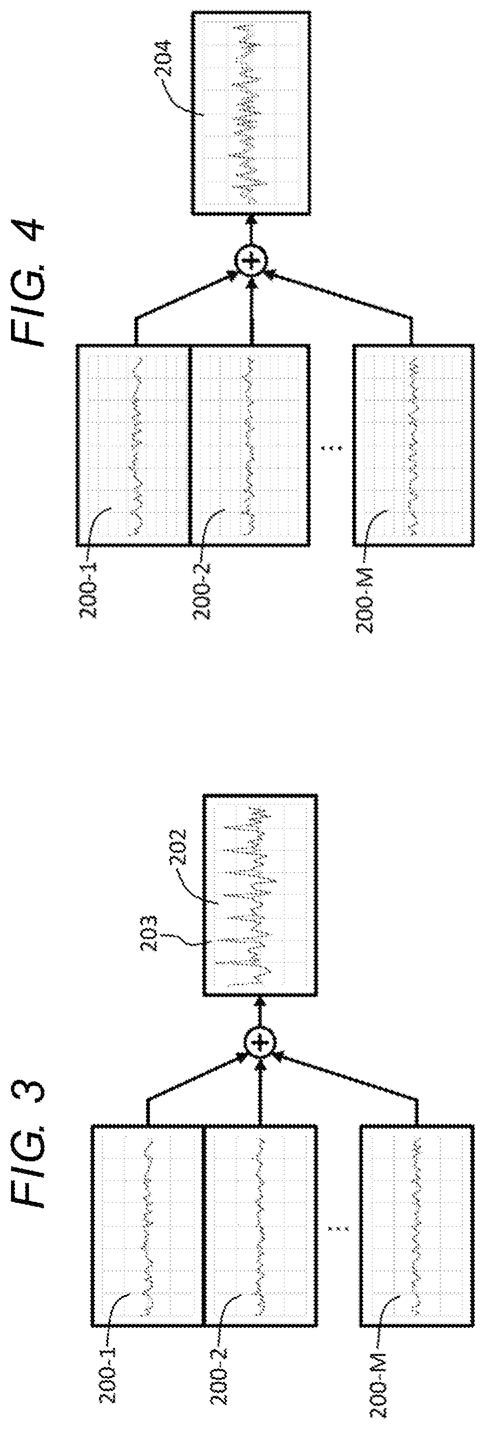
Such a noise may periodically occur due to the cyclic operation of the memory cell array, and may increase at the step of adding the plurality of reception signals, thereby degrading an S / N ratio.
When such a configuration is employed, another problem that the number of memory cells increases arises.

Method used


Image

  • Ultrasonic Diagnosis Device and Electronic Circuit
  • Ultrasonic Diagnosis Device and Electronic Circuit
  • Ultrasonic Diagnosis Device and Electronic Circuit

Examples


first embodiment

[0055]In the first embodiment, the reset data 86 is configured with M reset signals, and the M reset signals are applied to the M write control modules and the M read control modules. Each of the reset signals functions as a start trigger. M reset timings according to the M reset signals are made irregular, and it is possible to make the use starting stage number different in each delay circuit, by applying such M reset signals to the M write control modules and the M read control modules in parallel.

[0056]FIG. 6 illustrates an operation of the sub beamformer in the first embodiment. The M delay circuits (that is, M memory cell arrays) are included in the sub beamformer. Reference numeral 100 indicates a clock. Reference numeral 102-1 indicates a first reset signal, that is, a first start trigger, for regulating the operation of the first delay circuit. 102-2 indicates a first reset signal, that is, a first start trigger, for regulating the operation of the second delay circuit. Ref...

second embodiment

[0065]In the second embodiment, the reset signal 90 is one common signal with respect to the M delay circuits. On the other hand, the offset data 88 is configured with M offsets (offset signals), and the M offsets are applied to M write control modules and M read control modules in parallel.

[0066]FIG. 8 illustrates an operation of the sub beamformer in the second embodiment. As described above, a reset signal 102 is a common signal with respect to the M delay circuits (M memory cell arrays). In reality, the M delay circuits are synchronized in parallel and operates by using a reset pulse 106 of the reset signal 102 as a temporal reference.

[0067]Reference numeral 103-1 indicates a first offset (offset value: 0), reference numeral 103-2 indicates a second offset (offset value: 1), and reference numeral 103-M indicates an M-th offset (offset value: M−1). Each of the offsets is for regulating a delay amount of write starting timing from a reference time defined by a reset pulse. The fir...

third embodiment

[0075]In the third embodiment, wiring shift numbers (parameters for making irregularity), which will be described below, are randomly set over the plurality of sub arrays 15 (that is, the plurality of sub beamformers 154). In addition, wiring shift numbers are randomly set in each sub array 15 on the basis of the vibration element 14a. Symbols a to h shown in reference numerals 156 and 158 indicate wiring shift numbers which are different. 0 may be included as a wire shift number. In reality, when the memory cell array is configured with N memory cells, N−1 wiring shift numbers (numerical values of 1 to N−1) may be selected. Reference numeral 156 indicates a wiring shift number on the basis of an element. In the illustrated example, the wiring shift numbers are randomly set between the sub arrays and in the sub array. Reference numeral 158 indicates a wiring shift number in delaying and addition at the second stage when two-stage sub beamforming is performed. To prevent an increase ...


PUM


Abstract

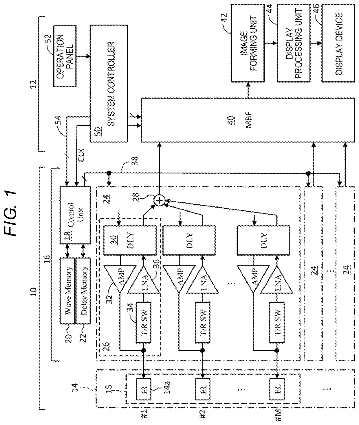
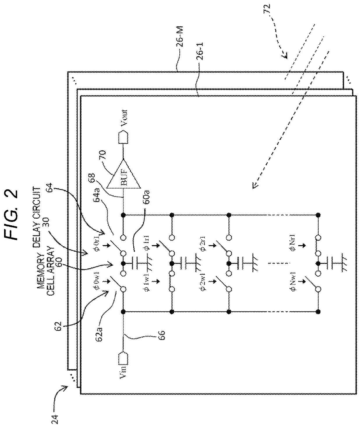
An electronic circuit in an ultrasonic probe includes a plurality of sub beamformers and a control unit. Each sub beamformer includes M delay circuits and an adding circuit. Each delay circuit includes a memory cell array which is formed of N memory cells. Conditions of cyclic operations of the M memory cell arrays (for example, timings of start triggers) are made irregular, such that use starting stage numbers in the M memory cell arrays are different.

Description

BACKGROUND OF THE INVENTION1. Field of the Invention[0001]The present invention relates to an ultrasonic diagnosis device and an electronic circuit, and more particularly, to delay processing in an ultrasonic probe.2. Description of Related Art[0002]An ultrasonic probe (3D probe) provided with a two dimensional vibration element array is used to obtain volume data by two-dimensionally scanning with an ultrasonic beam. In general, an electronic circuit is installed in the 3D probe, and the electronic circuit includes a plurality of sub beamformers to execute sub beamforming. Each sub beamformer includes a plurality of delay circuits and an adding circuit, and, after a plurality of reception signals are delay-processed in the plurality of delay circuits, the plurality of reception signals after being delay-processed are added at the adding circuit. The plurality of reception signals output from the plurality of sub beamformers are output to a device main body. In the above description...

Claims


Application Information

Patent Timeline
Patent Type & Authority Applications(United States)
IPC IPC(8): A61B8/00A61B8/08G01S7/52
CPCA61B8/4444A61B8/52G01S7/5208A61B8/54G01S7/52077A61B8/565G01S15/8925G01S15/8927G01S7/52026A61B8/488A61B8/12
Inventor KANEKO, TAKUYAKAJIYAMA, SHINYA
Owner FUJIFILM HEALTHCARE CORP
Learn More