

Integrated structures of acoustic wave device and varactor, and acoustic wave device, varactor and power amplifier, and fabrication methods thereof
a technology of integrated structures and acoustic waves, applied in the direction of amplifiers with semiconductor devices/discharge tubes, solid-state devices, basic electric elements, etc., can solve the problems of high materials cost, high equipment cost, time-consuming, etc., and achieve the effect of widening the gap, reducing component size, and optimizing impedance matching
- Summary
- Abstract
- Description
- Claims
- Application Information
AI Technical Summary
Benefits of technology
Problems solved by technology
Method used
Image

Examples
Embodiment Construction
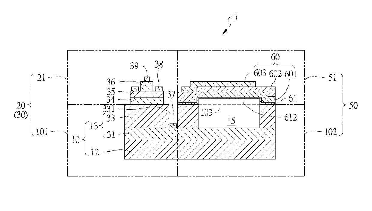
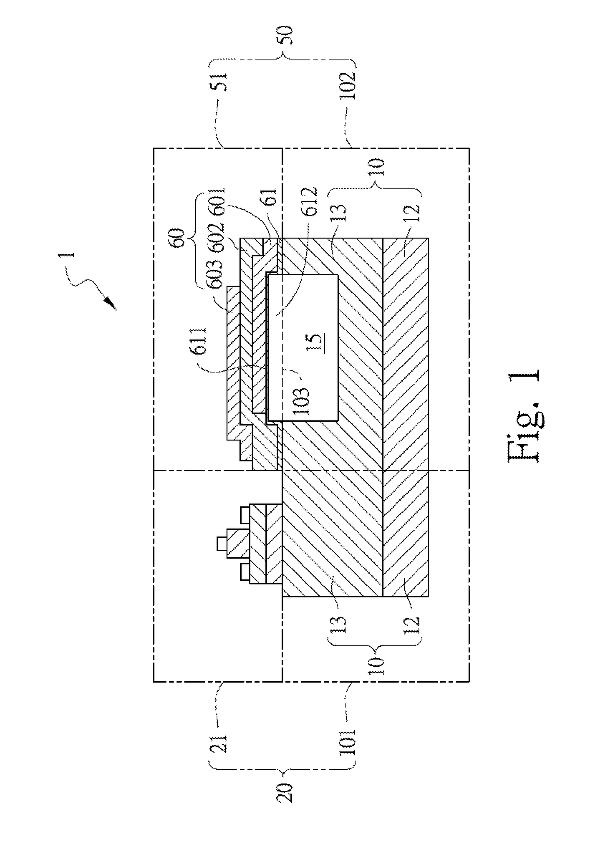
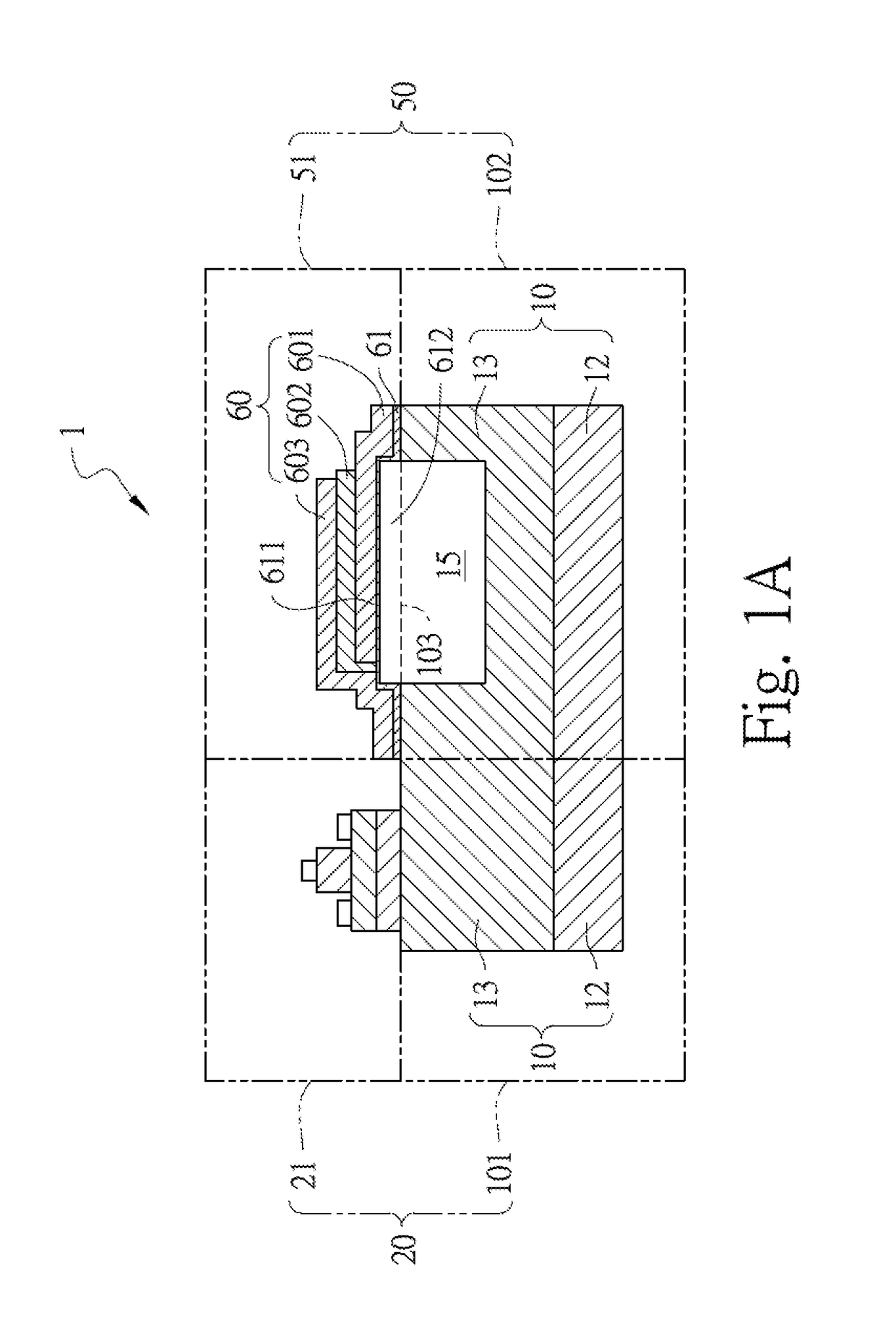
[0121]Please refer to FIG. 1, the cross-sectional view of an embodiment of the integrated structure of power amplifier and acoustic wave device of the present invention, the integrated structure comprises: a compound semiconductor epitaxial substrate 10, a power amplifier upper structure 21 and a film bulk acoustic resonator 51. The compound semiconductor epitaxial substrate 10 includes a compound semiconductor substrate 12 and an epitaxial structure 13 formed on the compound semiconductor substrate 12. The power amplifier upper structure 21 is formed on a first side 101 of the compound semiconductor epitaxial substrate 10, wherein the first side 101 of the compound semiconductor epitaxial substrate 10 and the power amplifier upper structure 21 form a power amplifier 20. The film bulk acoustic resonator 51 is formed on a second side 102 of the compound semiconductor epitaxial substrate 10, wherein the second side 102 of the compound semiconductor epitaxial substrate 10 and the film ...
PUM
 Abstract
Description
Claims
Application Information