Manufacturing method of semiconductor device

a manufacturing method and semiconductor technology, applied in the direction of fluid pressure measurement, fluid pressure measurement by electric/magnetic elements, instruments, etc., can solve the problems of failure to reach the intended pressure, the pressure in the airtight chamber may become higher than the intended pressure, and the difficulty of similar difficulties also arises. , the effect of restricting the generation of hydrogen gas and restricting the fluctuation of the pressure caused by hydrogen gas

Active Publication Date: 2018-04-17
DENSO CORP
View PDF13 Cites 0 Cited by
  • Summary
  • Abstract
  • Description
  • Claims
  • Application Information

AI Technical Summary

Benefits of technology

[0012]In the heat treatment, the OH groups left in the airtight chamber 30 are completely converted into the hydrogen gas. Thus, in the airtight chamber 30, the generation of the hydrogen gas can be restricted and the fluctuation in the pressure caused by the hydrogen gas can be restricted when the semiconductor device is in use.

Problems solved by technology

Though the above-described method using chemical bond can enhance the strength of joining between the first substrate and the second substrate, there is a difficulty that a pressure in the airtight chamber becomes higher than an intended pressure due to hydrogen gas (that is, degassing) which is generated in the airtight chamber from the OH groups.
When the heat treatment is not performed adequately, the pressure in the airtight chamber may fail to reach an intended pressure.
A similar difficulty also arises, for example, in a pressure sensor or the like having the airtight chamber as a reference pressure chamber when the airtight chamber is provided by joining the first substrate and the second substrate together.

Method used


Image

  • Manufacturing method of semiconductor device
  • Manufacturing method of semiconductor device
  • Manufacturing method of semiconductor device

Examples


first embodiment

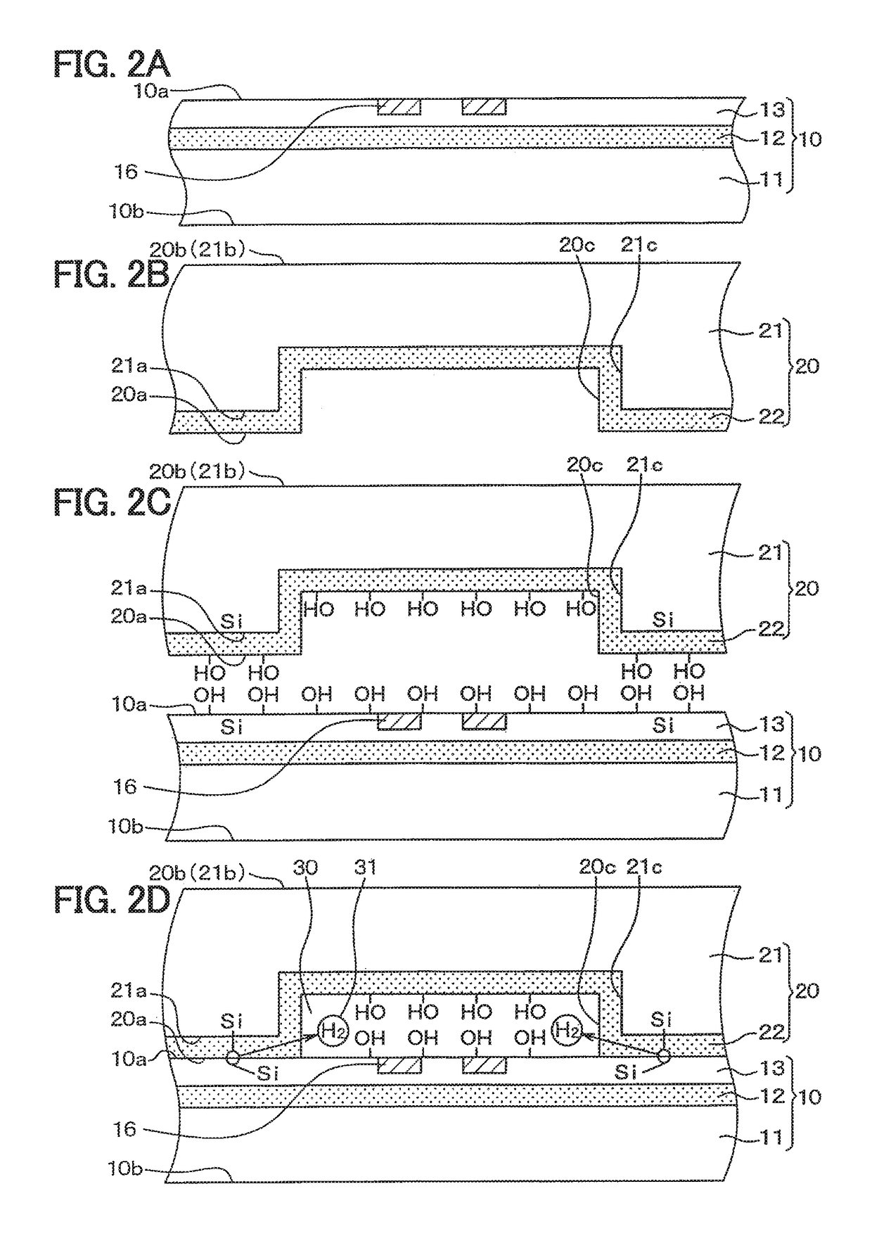
[0023]The following will describe a first embodiment of the present disclosure with reference to the drawings. The present embodiment will describe an example in which a manufacturing method of a semiconductor device according to the present disclosure is applied to a manufacturing method of a pressure sensor. The following will describe a pressure sensor manufactured by the manufacturing method according to the present embodiment.

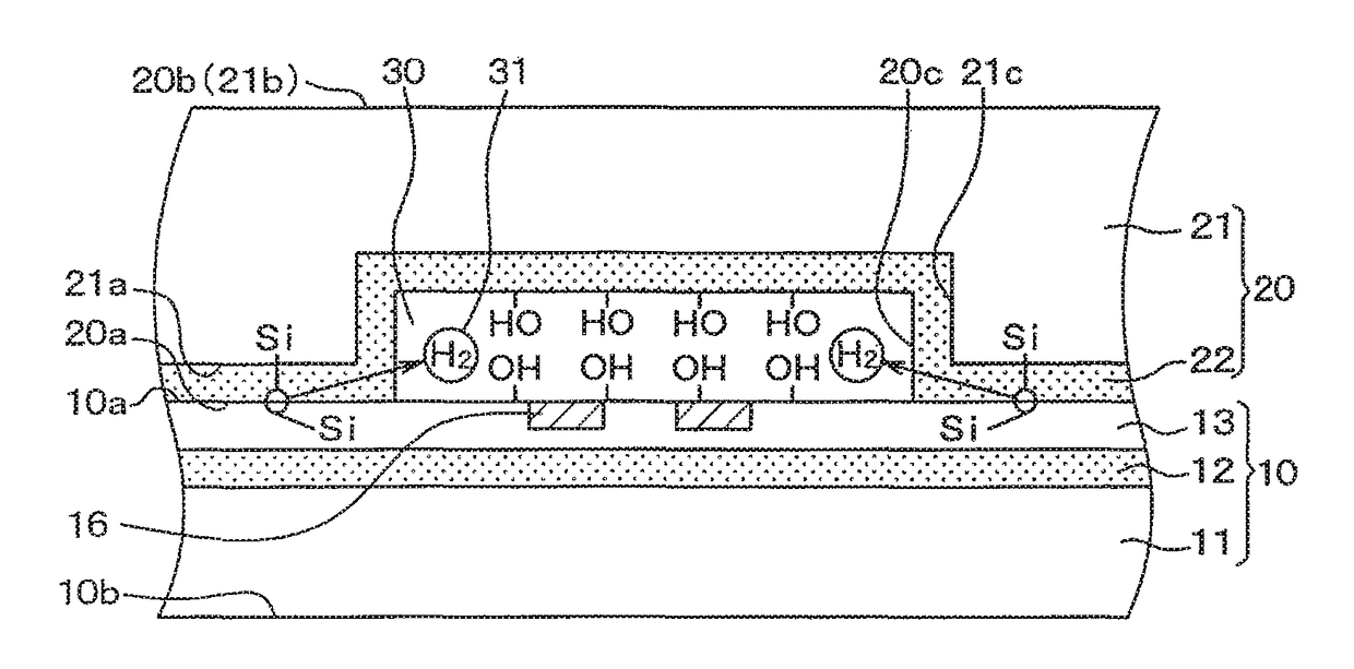
[0024]As shown in FIG. 1, the pressure sensor in the present embodiment includes a first substrate 10, and the first substrate 10 has one surface 10a and another surface 10b. In the present embodiment, the first substrate 10 is configured by an SOI (Silicon on Insulator) in which a supporting substrate 11, an insulating film 12, and a semiconductor layer 13 are stacked in described order. Thus, the one surface 10a of the first substrate 10 is provided by one surface of the semiconductor layer 13, which is arranged opposite to the insulating film 12. Anothe...

second embodiment

[0061]The second embodiment of the present disclosure will be described. The present embodiment is obtained by modifying the configuration of the first substrate 10 in the first embodiment. The present embodiment is similar to the first embodiment, and a description of the similar or same portion is omitted hereinafter for simplification.

[0062]As shown in FIG. 6, in the pressure sensor in the present embodiment, the first substrate 10 has a thin insulating film 17 on the semiconductor layer 13. That is, the first substrate 10 includes the supporting substrate 11, the insulating film 12, the semiconductor layer 13, and the thin insulating film 17 which are stacked in described order. The one surface 10a is provided by one surface of the thin insulating film 17, which is disposed on opposite side of the semiconductor layer 13. The diaphragm portion 15 is provided by partial insulating film 12, partial semiconductor layer 13, and partial thin insulating film 17 which are disposed betwe...


PUM

PropertyMeasurementUnit
temperatureaaaaaaaaaa
lengthaaaaaaaaaa
distanceaaaaaaaaaa

Abstract

A manufacturing method of a semiconductor device, in which a vacuum-pressure airtight chamber is defined by a space between a first substrate and a recessed portion of a second substrate, includes preparing the first substrate and the second substrate both of which contain silicon, joining the two substrates together, performing a heat treatment to emit hydrogen gas from the airtight chamber, and generating OH groups on the substrates before the joining. In the joining of the substrates together, the OH groups are bonded together to generate covalent bonds, and in the heat treatment, a part on which the OH groups are generated is heated at a temperature rise rate of 1° C. / sec or smaller until a temperature of the substrate increases to 700° C. or higher, and a heating temperature and heating time are adjusted to emit hydrogen gas from the airtight chamber.

Description

CROSS REFERENCE TO RELATED APPLICATIONS[0001]This application is a U.S. national stage application of International Patent Application No. PCT / JP2016 / 000553 filed on Feb. 3, 2016 and is based on Japanese Patent Application No. 2015-27738 filed on Feb. 16, 2015 and Japanese Patent Application No. 2015-242400 filed on Dec. 11, 2015, the disclosures of which are incorporated herein by reference.TECHNICAL FIELD[0002]The present disclosure relates to a manufacturing method of a semiconductor device in which a first substrate and a second substrate are joined together to configure an airtight chamber between the first substrate and the second substrate.BACKGROUND ART[0003]Conventionally, a semiconductor device having an airtight chamber between a first substrate and a second substrate described below has been proposed (see, e.g., Patent Literature 1). In this semiconductor device, a sensing portion which detects an angle velocity is formed on the first substrate. In the second substrate, ...

Claims


Application Information

Patent Timeline
Patent Type & Authority Patents(United States)
IPC IPC(8): B81C1/00G01L9/00H01L21/20H01L21/18
CPCB81C1/00357G01L9/0042G01L9/0051H01L21/2007B81B2203/0127H01L21/187B81B2201/0264B81C1/00293H01L21/76251
Inventor HAYAKAWA, YUTAKAYOKURA, HISANORI
Owner DENSO CORP
Why Eureka
Try Eureka