

Method of forming tungsten film
- Summary
- Abstract
- Description
- Claims
- Application Information
AI Technical Summary
Benefits of technology
Problems solved by technology
Method used
Image

Examples
Embodiment Construction
[0056] Hereinafter, a preferred embodiment of a method of forming a tungsten film in accordance with the present invention will be described in detail with reference to the accompanying drawings.
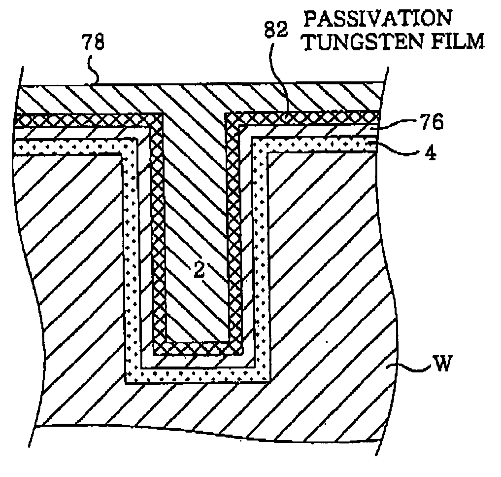
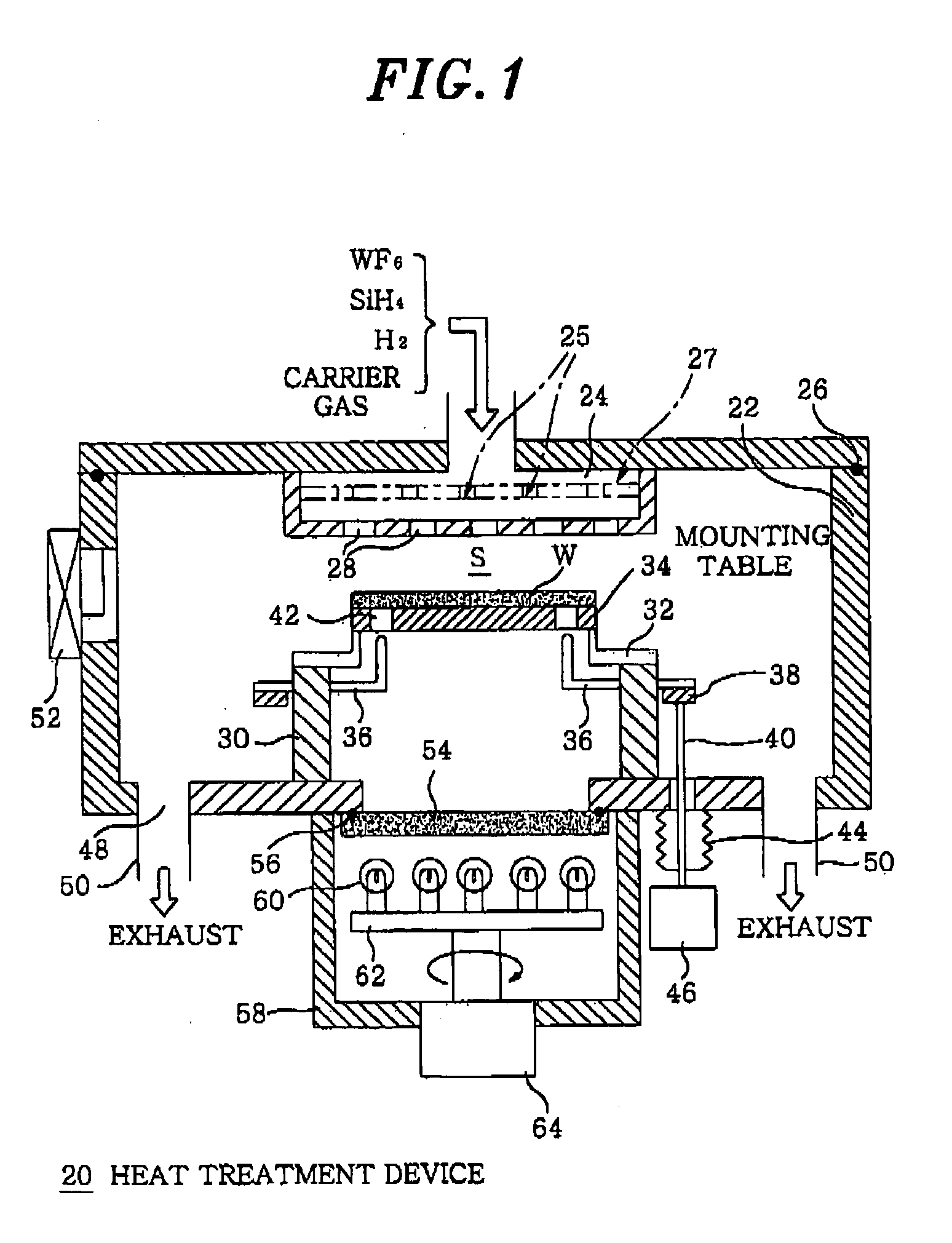
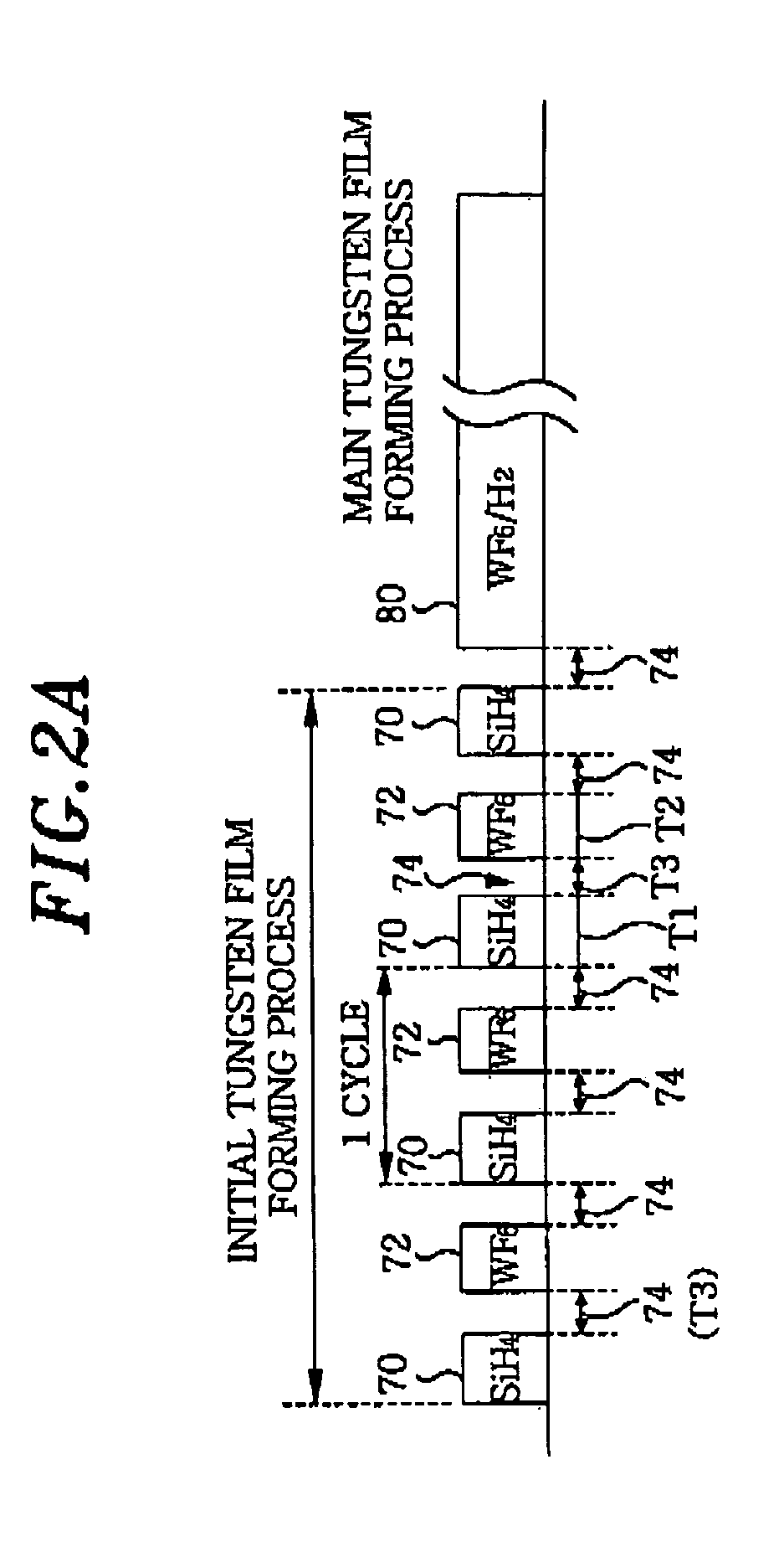
[0057]FIG. 1 is a cross sectional view of a heat treatment device for performing a method of forming a tungsten film in accordance with the present invention. FIGS. 2A to 2D provide supply patterns of each gas. FIG. 4 illustrates an enlarged cross sectional view of an exemplary tungsten film deposited on a semiconductor wafer surface. FIG. 5 presents an enlarged cross sectional view of another exemplary tungsten film deposited on a semiconductor wafer surface.
[0058] First of all, an explanation of a heat treatment device for performing the method of the present invention will be provided. The heat treatment device 20 has a processing vessel 22 having an approximately cylindrical cross-section, for example, which is made of aluminum. Installed on a ceiling portion of the processing vessel 2...
PUM
| Property | Measurement | Unit |
|---|---|---|
| Temperature | aaaaa | aaaaa |
| Thickness | aaaaa | aaaaa |
| Partial pressure | aaaaa | aaaaa |
Abstract
Description
Claims
Application Information