Electrooptical device, electrooptical device manufacturing method, and electronic apparatus

a manufacturing method and electrooptical technology, applied in the direction of semiconductor devices, electrical equipment, basic electric elements, etc., can solve the problems of short circuit between power supply lines and pixel electrodes, prone to defects on insulating films, and unstable light path lengths, so as to prevent defects

Active Publication Date: 2018-04-24
LUMITEK DISPLAY TECH LTD
View PDF15 Cites 1 Cited by
  • Summary
  • Abstract
  • Description
  • Claims
  • Application Information

AI Technical Summary

Benefits of technology

[0008]An advantage of some aspects of the embodiment is to provide an electro-optical device capable of preventing a defect on insulating films that are formed between reflection layers and pixel electrodes from being generated when the reflection layers are provided for respective pixels, an electro-optical device manufacturing method, and an electronic apparatus including the electro-optical device.
[0010]With the aspect of the embodiment, the light-reflective first conductive layers are arranged in both of the display region and the peripheral region as the region around the display region. The second conductive layers are arranged in both of the display region and the peripheral region so as to overlap with the first conductive layers. Accordingly, the display region and the peripheral region have the same pattern density and uniformity of etching of the insulating layers is improved. As a result, generation of defects on the insulating layers is suppressed. Furthermore, the cathode potential or the ground potential is applied to the first conductive layers arranged in the peripheral region. Therefore, even if the defects on the insulating layers are generated, the first conductive layers arranged in the peripheral region have the cathode potential or the ground potential and light emission of pixels can thereby be suppressed.
[0012]The electro-optical device in the above-described aspect of the embodiment may further include a fourth conductive layer to which a ground potential is applied, wherein the fourth conductive layer is electrically connected to the portion of the first conductive layers arranged in the peripheral region. With the aspect of the embodiment, even if the defects on the insulating layers are generated and the second conductive layers and the first conductive layers are electrically connected to each other, the second conductive layers have the ground potential and light emission of the pixels can thereby be suppressed.
[0013]The electro-optical device in the above-described aspect of the embodiment may further include an etching stop layer between the insulating layers and the first conductive layers, wherein the etching stop layer overlaps with end portions of the insulating layers when seen from the above. With the aspect of the embodiment, the etching stop layer overlaps with the end portions of the insulating layers when seen from the above. Therefore, even when another insulating layers are further laminated on the insulating layers, etching can be performed without influencing the first conductive layer under the etching stop layer.
[0015]With the aspect of the embodiment, the light-reflective first conductive layers are arranged in both of the display region and the peripheral region as the region around the display region. The second conductive layers are arranged in both of the display region and the peripheral region so as to overlap with the first conductive layers. Accordingly, the display region and the peripheral region have the same pattern density and uniformity of etching of the insulating layers is improved. As a result, generation of defects on the insulating layers is suppressed. Furthermore, the cathode potential or the ground potential is applied to the first conductive layers arranged in the peripheral region. Therefore, even if the defects on the insulating layers are generated, the first conductive layers arranged in the peripheral region have the cathode potential or the ground potential and light emission of pixels can thereby be suppressed.

Problems solved by technology

In such a case, defects on insulating films that are formed between the power supply line as the reflection layer and the pixel electrodes may cause the power supply line and the pixel electrodes to be short-circuited.
For example, the defects on the insulating films tend to be generated on the boundary between the display region and the adjacent region around the display region.
Furthermore, due to lowering in the uniformity of the etching of the insulating films, the light path lengths are not stable and desired wavelengths cannot be obtained in the pixels in some cases.

Method used


Image

  • Electrooptical device, electrooptical device manufacturing method, and electronic apparatus
  • Electrooptical device, electrooptical device manufacturing method, and electronic apparatus
  • Electrooptical device, electrooptical device manufacturing method, and electronic apparatus

Examples


Embodiment Construction

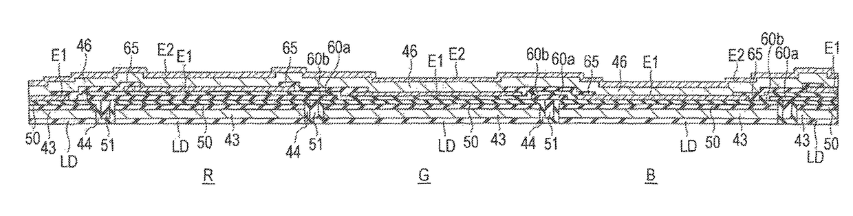
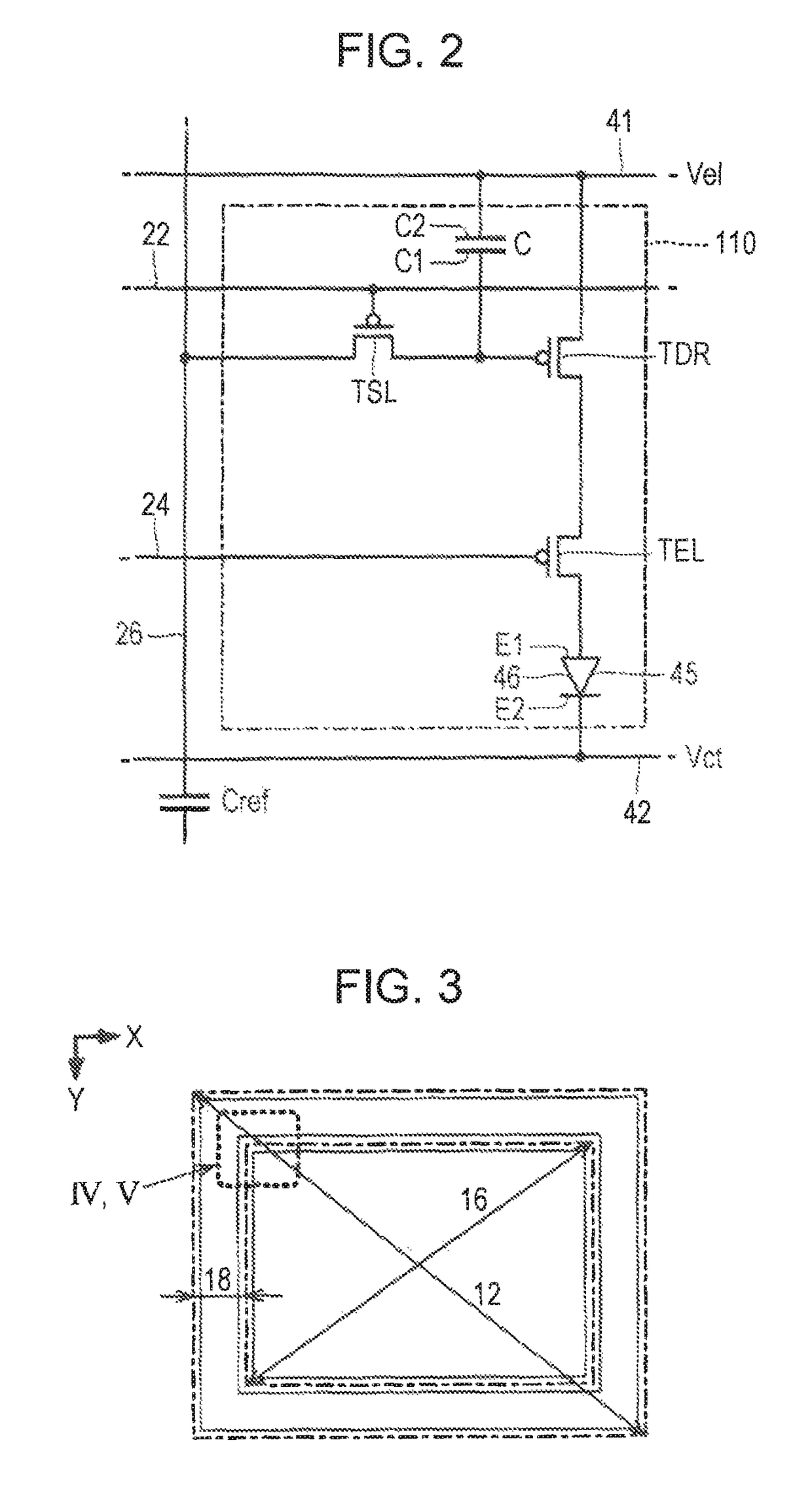
[0034]An embodiment will be described with reference to the drawings. It should be noted that in the following drawings, scales are made different for respective layers and respective members in order to make the layers and the members have sizes capable of being recognized in the drawings.

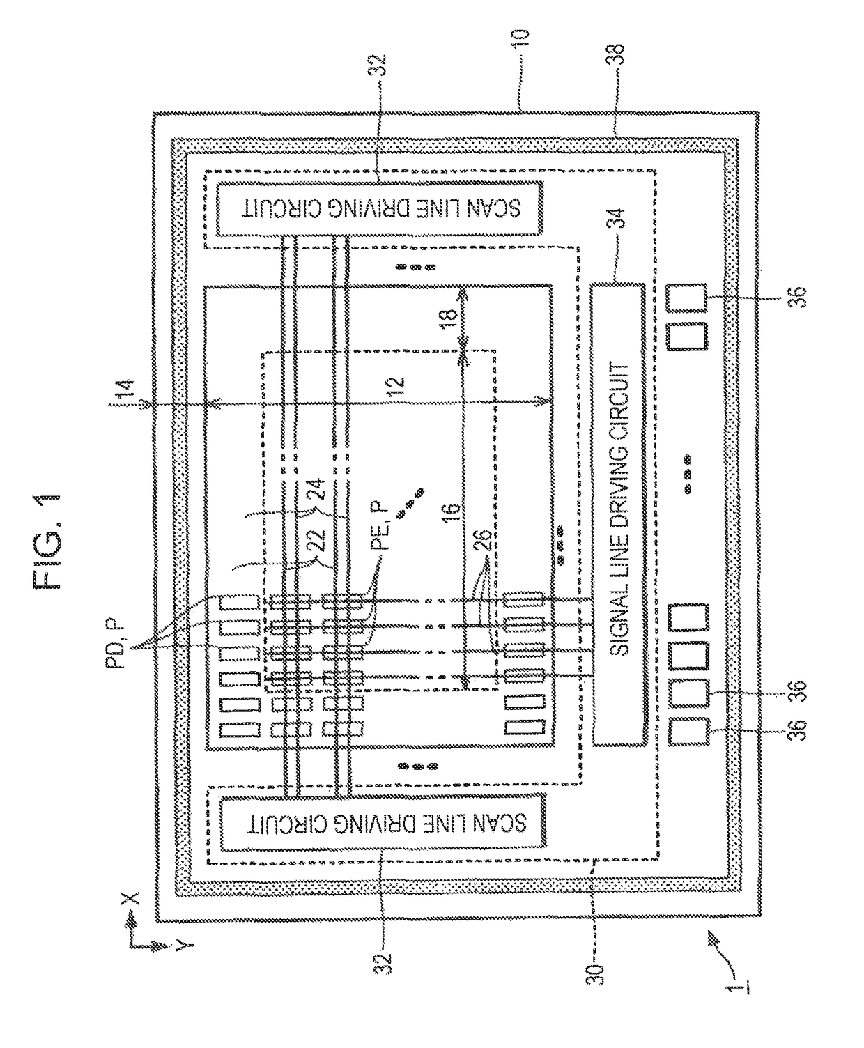
[0035]FIG. 1 is a plan view illustrating an electro-optical device 1 according to an embodiment. The electro-optical device 1 in the embodiment is an organic electroluminescence (EL) device in which light emitting elements using an organic EL material are formed on the surface of a substrate 10. The substrate 10 is a plate-like member (semiconductor substrate) formed with a semiconductor material such as silicon and is used as a base member (base) on which the plurality of light emitting elements are formed. As illustrated in FIG. 1, the surface of the substrate 10 is divided into a first region 12 and a second region 14. The first region 12 is a rectangular region and the second region 14 is a re...


PUM


Abstract

Reflection layers are arranged for respective pixels with predetermined intervals in a row direction (X direction) and a column direction (Y direction) in a display region, and, subsequently to the display region, are arranged in the same manner with the predetermined intervals in the row direction (X direction) and the column direction (Y direction) also in a peripheral region around the display region. First electrodes, first light path adjusting layers, and second light path adjusting layers are arranged for the respective pixels in the display region, and are arranged so as to correspond to the respective reflection layers also in the peripheral region. The respective reflection layers are partially connected to each other in the peripheral region and are electrically connected to a second electrode at a cathode potential.

Description

BACKGROUND[0001]1. Technical Field[0002]The present disclosure relates to an electro-optical device, an electro-optical device manufacturing method, and an electronic apparatus.[0003]2. Related Art[0004]In recent years, an electro-optical device using organic light emitting diodes (OLED) as light emitting elements has been used in an electronic apparatus capable of forming a virtual image, such as a head mount display. As an example of the electro-optical device, as disclosed in JP-A-2015-62194, a device that includes reflection layers for respective pixels and adjusts light paths based on optical distances between the reflection layers and pixel electrodes with cavity structures has been proposed.[0005]Furthermore, JP-A-2006-18085 discloses an electro-optical device in which pixels are arrayed in a display region displaying an image and dummy pixels that do not contribute to display of the image actually are arrayed in an adjacent region around the display region. The pixels in the...

Claims


Application Information

Patent Timeline
Patent Type & Authority Patents(United States)
IPC IPC(8): H01L27/32H01L51/52
CPCH01L27/3276H01L51/5271H10K50/856H10K59/131
Inventor KOSHIHARA, TAKESHIOTA, HITOSHI
Owner LUMITEK DISPLAY TECH LTD
Why Eureka
Try Eureka