Display device and method for driving same with light-emission enable signal switching unit

a technology of light-emission enabler and display device, which is applied in the direction of static indicating devices, instruments, etc., can solve the problems of difficult to achieve size increase and definition improvement, and difficult to achieve definition improvement, so as to reduce picture frame size, the effect of reducing the number of components and miniaturizing the display devi

Active Publication Date: 2018-05-01
SHARP KK
View PDF22 Cites 3 Cited by
  • Summary
  • Abstract
  • Description
  • Claims
  • Application Information

AI Technical Summary

Benefits of technology

[0077]According to the first aspect of the present invention, in a display device configured to be provided with a light-emission enable signal generating unit that generates a light-emission enable signal for controlling the on / off states of j light-emission control transistors which are provided in a one-to-one correspondence with j electro-optical elements (j is an integer greater than or equal to 3) in a pixel circuit; and j light-emission control lines for supplying the light-emission enable signal to each of the j light-emission control transistors, the light-emission enable signal generated by the light-emission enable signal generating unit is supplied to different light-emission control lines in different subframes by a light-emission enable signal switching unit. Since such a light-emission enable signal switching unit is provided, it is only necessary to generate one light-emission enable signal for each row. Therefore, the number of components (typically, drivers) for generating a light-emission enable signal can be reduced over conventional devices. By this, picture-frame size can be reduced over conventional devices, achieving miniaturization of a display device.
[0078]According to the second aspect of the present invention, as components for controlling the on / off states of j light-emission control transistors included in each pixel circuit, there are required a light-emission enable signal generating unit for only one system and j light-emission enable signal supply control transistors for each row. On the other hand, according to the conventional art, there are required light-emission enable signal generating units for j systems. The light-emission enable signal generating unit includes at least six transistors, and thus, according to the second aspect of the present invention, the transistor occupied area is reduced over conventional devices. Therefore, picture-frame size can be reduced over conventional devices, achieving miniaturization of a display device.
[0079]According to the third aspect of the present invention, thin-film transistors each having a channel layer formed of an oxide semiconductor are used. Hence, miniaturization of transistors is possible, enabling to more easily miniaturize a display device.
[0080]According to the fourth aspect of the present invention, by using indium gallium zinc oxide as the oxide semiconductor forming the channel layer, the effect of the third aspect of the present invention can be securely attained.
[0081]According to the fifth aspect of the present invention, in a display device configured such that the light-emission enable signal generating unit includes a shift register having a plurality of stages (unit circuits) each including six transistors, picture-frame size can be reduced over conventional devices.
[0082]According to the sixth aspect of the present invention, in each subframe, in j pixel circuits included in each group, electro-optical elements with different light-emitting colors go into a light-emitting state. That is, in each subframe, there are mixed light-emitting colors. By this, the occurrence of color breakup which is likely to occur when time-division driving (field sequential driving) is adopted is suppressed. By the above, a display device is implemented, in which picture-frame size is reduced over conventional devices while the occurrence of color breakup is suppressed.

Problems solved by technology

An organic EL display device adopting the passive matrix system is simple in structure, but is difficult to achieve size increase and definition improvement.
According to the configuration shown in FIG. 39, since many circuit elements are required within a pixel circuit, it is difficult to achieve definition improvement.

Method used


Image

  • Display device and method for driving same with light-emission enable signal switching unit
  • Display device and method for driving same with light-emission enable signal switching unit
  • Display device and method for driving same with light-emission enable signal switching unit

Examples


first embodiment

1. First Embodiment

1.1 Overall Configuration and Summary of Operation

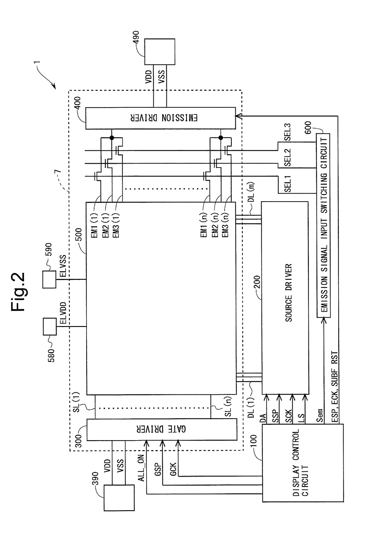
[0131]FIG. 2 is a block diagram showing an overall configuration of an active matrix-type organic EL display device 1 according to a first embodiment of the present invention. The organic EL display device 1 includes a display control circuit 100, a source driver (data line drive circuit) 200, a gate driver (scanning signal line drive circuit) 300, an emission driver 400, a display unit 500, and an emission signal input switching circuit 600. Note that the gate driver 300 and the emission driver 400 are formed in an organic EL panel 7 including the display unit 500 in the present embodiment. That is, the gate driver 300 and the emission driver 400 are monolithic. In addition, the organic EL display device 1 is provided with a logic power supply 390, a logic power supply 490, an organic EL high-level power supply 580, and an organic EL low-level power supply 590, as components for supplying various types of power su...

second embodiment

2. Second Embodiment

[0199]A second embodiment of the present invention will be described. Note that only differences from the above-described first embodiment will be described, and description of the same things as those of the above-described first embodiment is omitted. This also applies to a third embodiment and a fourth embodiment which will be described later.

[0200]

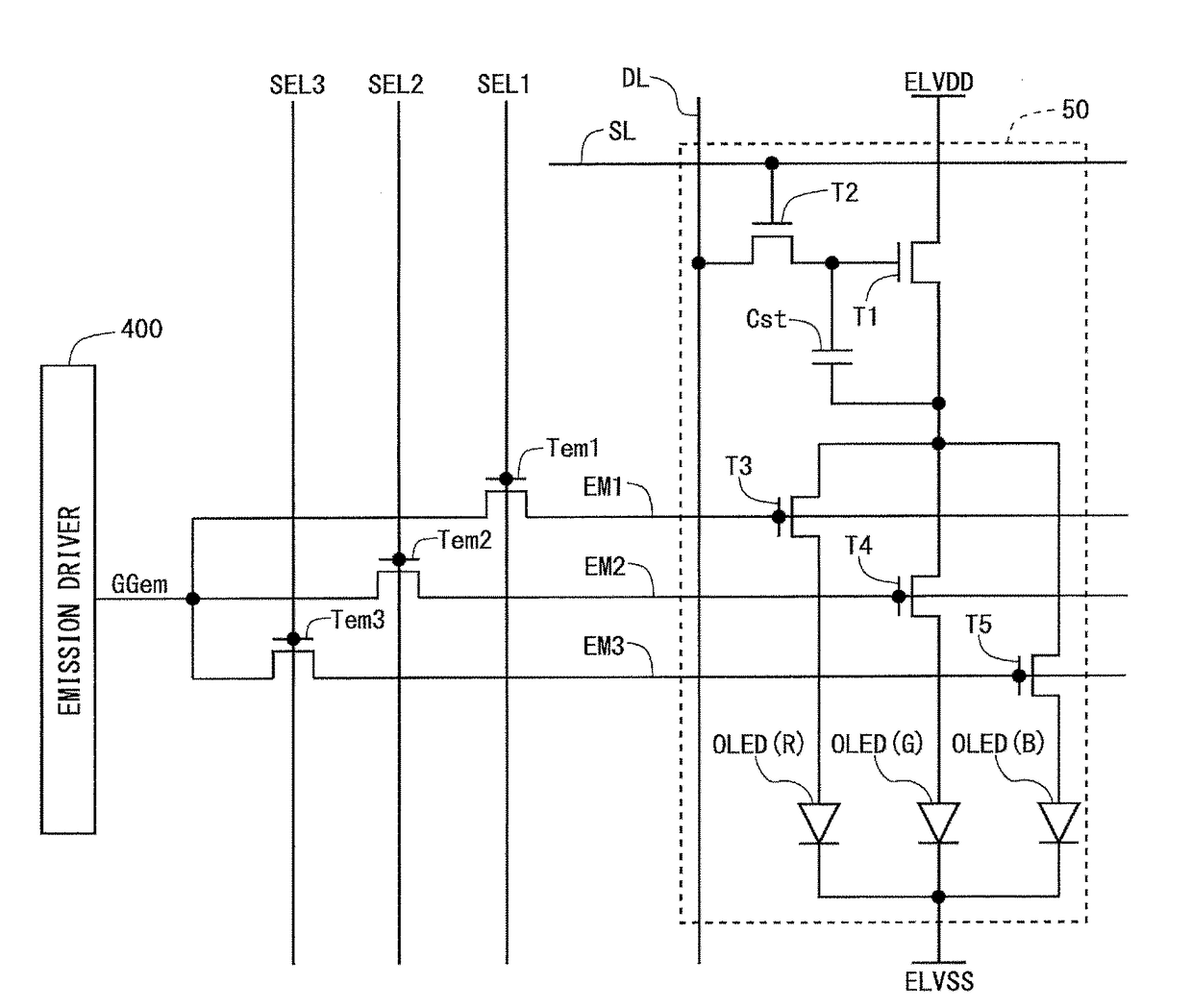
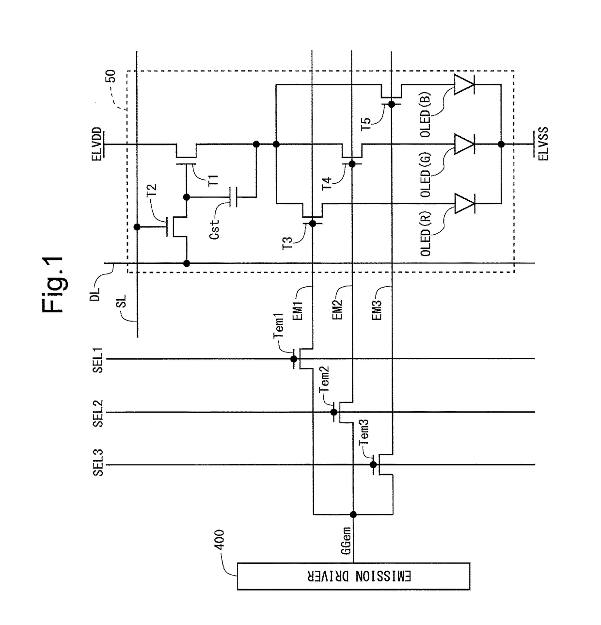
[0201]In the present embodiment, three pixel circuits 50 arranged side by side in a direction in which scanning signal lines SL extend are defined as one group. Since the number of columns is m, (m / 3) groups are formed for each row. FIG. 21 is a circuit diagram showing configurations of three pixel circuits 50(1) to 50(3) included in one group. The configuration of each pixel circuit 50 is the same as that of the above-described first embodiment (see FIG. 7). Here, a connection relationship between first to third emission lines EM1 to EM3 and the gate terminals of transistors T3 to T5 included in the three pixel cir...

third embodiment

3. Third Embodiment

3.1 Overall Configuration

[0209]FIG. 26 is a block diagram showing an overall configuration of an active matrix-type organic EL display device 2 according to a third embodiment of the present invention. In the present embodiment, unlike the above-described first embodiment (see FIG. 2), one demultiplexer DM is provided for each row between an emission driver 400 and emission lines EM. That is, n demultiplexers DM(1) to DM(n) are provided overall. Two selection signals (a selection signal CTL1 and a selection signal CTL2) are provided to each demultiplexer DM from an emission signal input switching circuit 600. In the present embodiment, a second control signal generating unit is implemented by the emission signal input switching circuit 600, and a second control signal is implemented by the selection signal CTL1 and the selection signal CTL2. Note that in the present embodiment high-mobility transistors using LTPS (low-temperature polysilicon) or C—Si (crystalline ...


PUM


Abstract

A picture-frame size of a display device including self light-emitting type display elements which are driven by a current is reduced over conventional devices. Transistors for controlling supply of a light-emission enable signal outputted from an emission driver to emission lines are provided between the emission driver and the emission lines. In such a configuration, based on selection signals provided to the transistors, one of the transistors is brought into an on state in each subframe, and each of the transistors is brought into an on state once during one frame period.

Description

TECHNICAL FIELD[0001]The present invention relates to a display device and more particularly to a display device including self light-emitting type display elements which are driven by a current, such as an organic EL display device, and a method for driving the display device.BACKGROUND ART[0002]Conventionally, as display elements included in a display device, there are an electro-optical element whose luminance is controlled by a voltage applied thereto, and an electro-optical element whose luminance is controlled by a current flowing therethrough. A representative example of the electro-optical element whose luminance is controlled by a voltage applied thereto includes a liquid crystal display element. On the other hand, a representative example of the electro-optical element whose luminance is controlled by a current flowing therethrough includes an organic EL (Electro Luminescence) element. The organic EL element is also called an OLED (Organic Light-Emitting Diode). An organic...

Claims


Application Information

Patent Timeline
Patent Type & Authority Patents(United States)
IPC IPC(8): G09G3/20G09G3/3233G09G3/3258G09G3/3266
CPCG09G3/2022G09G3/3233G09G3/3258G09G3/3266G09G3/2003G09G2330/021G09G2300/0443G09G2300/0452G09G2300/0804G09G2310/0235G09G2310/0286G09G2310/0289G09G2310/0291G09G2310/061G09G2310/08G09G2320/064
Inventor OHARA, MASANORINOGUCHI, NOBORUKISHI, NORITAKA
Owner SHARP KK
Why Eureka
Try Eureka