
High Q quartz-based MEMS resonators and methods of fabricating same

a quartz-based, high-q technology, applied in piezoelectric/electrostrictive device manufacture/assembly, electrical apparatus, etc., can solve the problems of inability to use soft masks to form lower frequency devices, large size and cost of the overall unit, and the use of soft masks in the u.s., so as to increase the yield of devices, reduce costs, and ensure the effect of stability

Active Publication Date: 2018-05-29
HRL LAB
View PDF14 Cites 2 Cited by
  • Summary
  • Abstract
  • Description
  • Claims
  • Application Information

AI Technical Summary

Benefits of technology

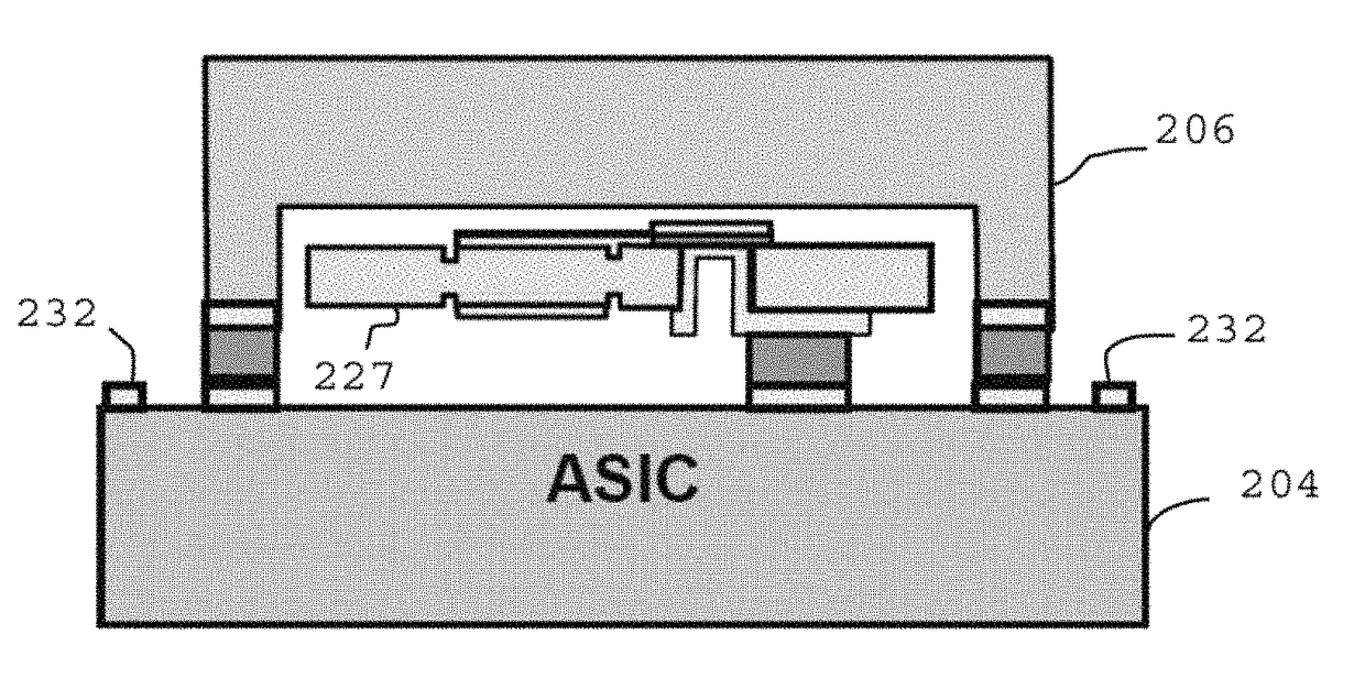
The present invention is a design for a thickness-shear mode quartz resonator that can be used to make oscillators for frequencies ranging from HF to UHF. The fabrication method includes a step of temporary attachment of the quartz device wafer to a quartz handle wafer using adhesive bonding for plasma dry etching. The method allows for high-Q operation with energy trapping / mode confinement. The resonators can be batch etched on a single quartz substrate and then released and transferred to a host substrate such as an oscillator ASIC to form a fully integrated monolithic crystal oscillator. The invention also introduces a novel quartz resonator temporary attachment and release technology that can increase device yield and lower cost. Overall, the invention improves the efficiency and precision of quartz resonator design and fabrication for a range of applications.

Problems solved by technology

Unfortunately, the soft mask cannot be used to form lower frequency devices.
Thus, the size and cost of the overall unit are significantly increased.
However, due to the vastly different quartz thickness between the UHF and lower frequency devices (several microns compared with several tens or hundreds of microns), the soft (photoresist) mask used in U.S. Pat. No. 7,237,315 can no longer be applied to this invention.

Method used


Image

  • High Q quartz-based MEMS resonators and methods of fabricating same
  • High Q quartz-based MEMS resonators and methods of fabricating same
  • High Q quartz-based MEMS resonators and methods of fabricating same

Examples


Embodiment Construction

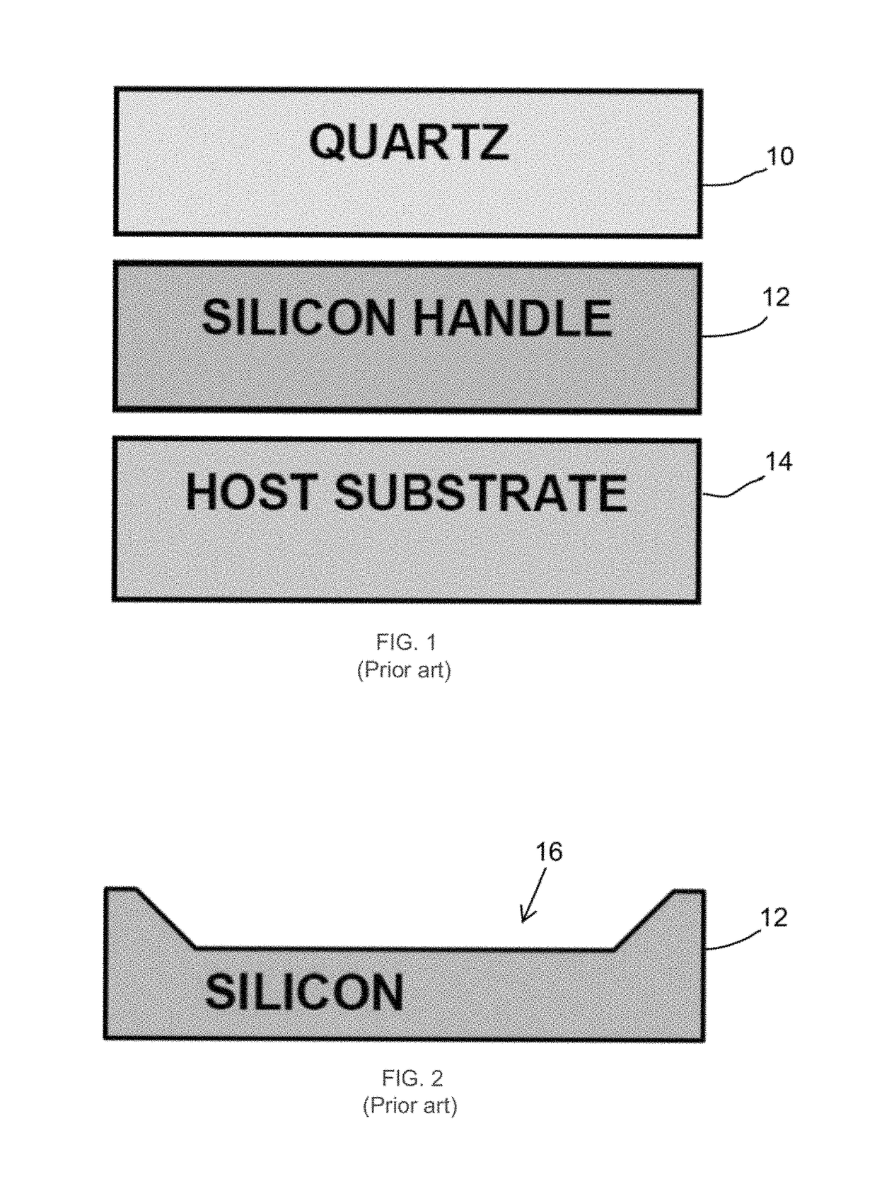
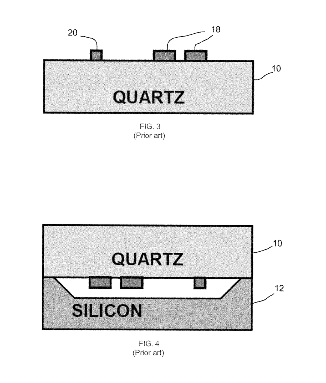
[0042]An exemplary fabrication process flow for an integrated quartz oscillator of the present invention is illustrated in cross-section in FIGS. 13-31. The starting materials, as shown in a side view in FIG. 13, consist of a quartz device wafer 200 (for the resonator), a handle wafer 202, a host substrate 204 (such as a silicon CMOS ASIC wafer with oscillator drive circuitry) and a silicon cap wafer 206 for hermetic sealing purpose. A quartz handle wafer is chosen instead of a silicon handle because the quartz handle offers better thermal matching to the quartz device wafer. The specific ASIC host substrate design provided herein is exemplary only and other configurations are within the scope of the present invention. In this embodiment, the handle wafer is made of quartz. In general, it is desirable that the handle wafer is formed of materials that have a coefficient of thermal expansion within a range from 0.5 to 12 ppm / degree C. Exemplary materials include crystalline quartz, fu...


PUM


Abstract

High-yield fabrication methods are provided for making quartz resonators having thicknesses ranging from one micrometer to several hundred micrometers and thus covering the frequency range from HF to UHF. Plasma dry etching is used to form arbitrary resonator geometries. The quartz resonator structure and the through-quartz vias are formed concurrently. The method includes bonding a quartz device wafer to a quartz handle wafer with a temporary adhesive. Mesa structures formed by plasma dry etching enable the resonators to achieve high-Q operation with energy trapping / mode confinement. A thermo-compression bond integrates the quartz resonators to a host wafer (e.g., an oscillator ASIC) to form oscillators. Silicon cap wafers are bonded over the resonators to the ASIC to provide wafer scale hermetic encapsulation of the quartz oscillators.

Description

CROSS-REFERENCE TO RELATED APPLICATIONS[0001]This is a continuation-in-part of U.S. patent application Ser. No. 12 / 816,292, titled “Quartz-Based MEMS Resonators and Method of Fabricating Same,” filed Jun. 15, 2010, incorporated herein by reference.STATEMENT REGARDING FEDERALLY SPONSORED RESEARCH OR DEVELOPMENT[0002]This invention was made with Government support under Contract No. 20071095726000 awarded by the U.S. Government. The Government has certain rights in the invention.BACKGROUNDField[0003]The present technology relates to thickness-shear mode quartz resonators, and more specifically, it relates to high Q quartz-based MEMS resonators operating at HF-UHF band frequencies.Description of Related Art[0004]A process for manufacturing a quartz-based nanoresonator was provided in U.S. Pat. No. 7,237,315, titled “Method for Fabricating a Resonator,” incorporated herein by reference. U.S. Pat. No. 7,237,315 addresses VHF to UHF frequency devices that have less than 10 μm of quartz th...

Claims


Application Information

Patent Timeline
IPC IPC(8): H01L41/311H01L41/047H01L41/053H01L41/23H01L41/332H01L41/29
CPCH01L41/311H01L41/053H01L41/0475H01L41/23H01L41/29H01L41/332H03H3/02H03H9/1021H03H9/19H03H2003/022
Inventor CHANG, DAVID T.STRATTON, FREDERIC P.NGUYEN, HUNGKUBENA, RANDALL L.
Owner HRL LAB
Learn More