Apparatus for stacking semiconductor chips

a technology of semiconductor chips and apparatus, applied in the direction of electrical apparatus construction details, solid-state devices, basic electric elements, etc., can solve the problems of many techniques not using surface mount technology, a number of defects, etc., and achieve the effect of increasing the density of memory chips and increasing the density of components

Inactive Publication Date: 2000-10-17
HGST TECH SANTA ANA
View PDF96 Cites 126 Cited by
  • Summary
  • Abstract
  • Description
  • Claims
  • Application Information

AI Technical Summary

Benefits of technology

The present invention involves a multi-chip memory module having two or more vertically stacked memory chips that are interconnected using a pair of printed circuit boards or "side boards." The multi-chip memory module can be constructed using standard, off-the-shelf memory chips, without modification to the pins of the memory chips. The multi-chip memory module is constructed such that pins of the lower-most memory chip in the stack are surface-mountable directly to pads of a memory board, permitting the multi-chip memory module to be mounted with a low profile relative to the memory board.
In accordance with an additional aspect of the invention, there is provided a method of increasing the density of memory chips on a memory board. The method includes the step of providing first and second side boards, with each side board comprising a printed circuit board having vias thereon, and with vias along bottom edges of the side boards forming surface mount terminals. The method further includes the step of stacking a plurality of memory chips on top of one another to generate a stack of memory chips. The method further includes the steps of positioning the first and second side boards relative to the stack of memory chips such that terminals of the memory chips extend within the vias, and attaching the first and second side boards to the stack of memory chips by filling the vias with solder.
In accordance with another aspect of the invention, there is provided a method of interconnecting circuit board components to increase component density. The method includes the step of constructing a first printed circuit board that has a plurality of vias formed along a row. The method further includes the step of cutting the first printed circuit board along the row to expose the vias along an edge of the printed circuit board. The method further includes the steps of soldering the vias to respective pins of a semiconductor chip, and soldering the vias to pads of a second printed circuit board such that the first printed circuit board is substantially perpendicular to the second printed circuit board.

Problems solved by technology

These techniques, however, tend to suffer from a number of defects.
Further, many of the techniques do not make use of the various advantages of surface mount technology, such as the ability to maintain a low-profile when memory chips are mounted to the printed circuit board.
Further, many proposed techniques for stacking memory chips are not cost effective.

Method used


Image

  • Apparatus for stacking semiconductor chips
  • Apparatus for stacking semiconductor chips
  • Apparatus for stacking semiconductor chips

Examples


Embodiment Construction

In accordance with one embodiment of the present invention, one multi-chip memory module design is described herein. In order to fully specify this

preferred design, various embodiment-specific details are set forth, such as the number of memory chips in the module, the layouts of the printed circuit boards of the module, and the capacity, number of data bits and pin-outs of the memory chips. It should be understood, however, that these details are provided only to illustrate this single preferred embodiment, and are not intended to limit the scope of the present invention.

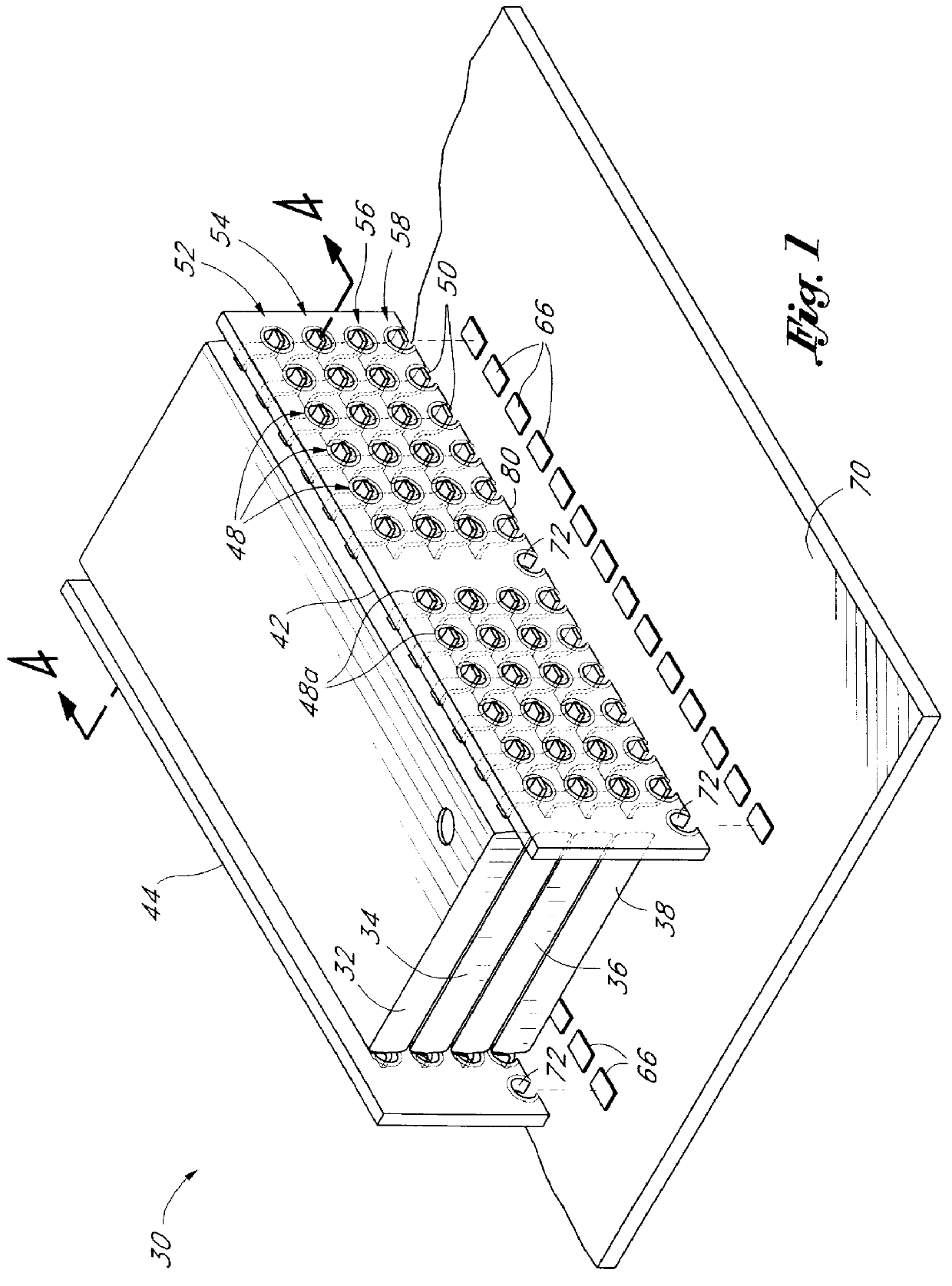
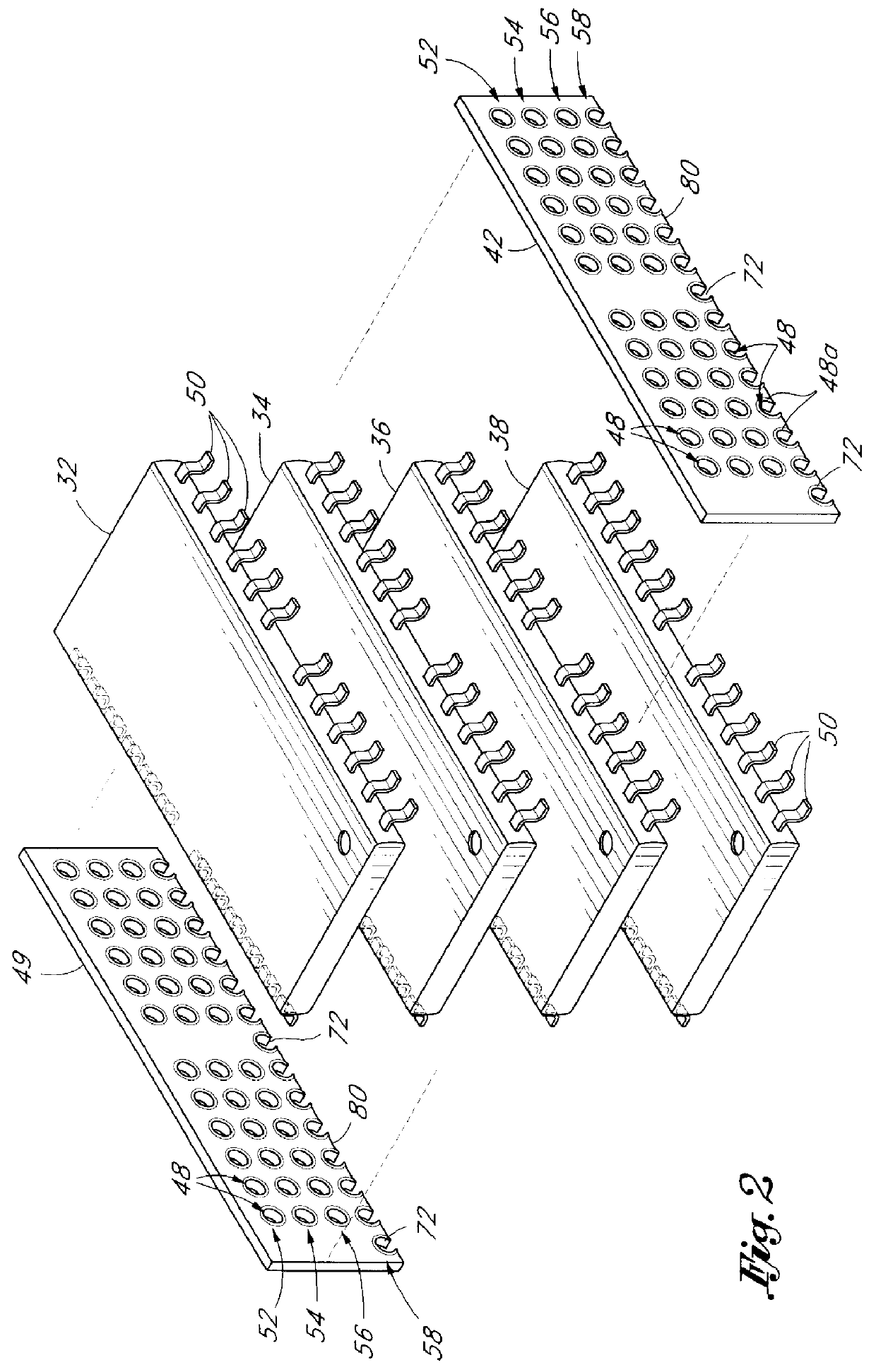
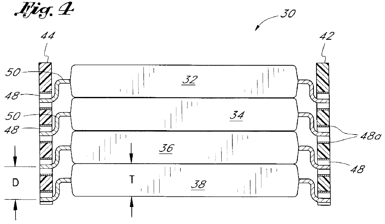
With reference to FIGS. 1-4, a 28-terminal multi-chip memory module 30 (hereinafter "multi-chip module") comprises four functionally-identical, vertically-stacked memory chips 32, 34, 36, 38. The memory chips 32-38 are conventional 24-pin surface mount TSOP ("thin small outline package") chips, available from Toshiba, Mitsubishi, and the like. Each memory chip 32-38 has a capacity of 16M.times.1-bit.

The vertically-...


PUM


Abstract

A multi-chip memory module comprises multiple standard, surface-mount-type memory chips stacked on top of each other, and a pair of printed circuit boards mounted on opposite sides of the memory chips to electrically interconnect the memory chips. Each printed circuit board has vias that are positioned to form multiple rows, with each row of vias used to connect the printed circuit board to a respective memory chip. The vias falling along the bottom-most row of each printed circuit board are also exposed and are used to surface mount the multi-chip module to pads of a memory board.

Description

BACKGROUND OF THE INVENTION1. Field of the InventionThe present invention relates to the vertical stacking of conventional integrated circuit packages to increase the density of components on a printed circuit board. More particularly, the present invention relates to the vertical stacking of conventional memory integrated circuits packages on a surface mount printed circuit board.2. Description of the Related ArtAn integrated circuit or "IC" is a microcircuit formed from active and passive electrical components interconnected on or within a single semiconductor substrate. To protect the IC and to facilitate connection of the IC to a printed circuit board, off-the-shelf ICs are commonly packaged within a ceramic, plastic or epoxy IC package having multiple external terminals or "pins." The full integrated circuit package, including the IC, is commonly referred to (and will be referred to herein) as a "chip."As a result of the continuously increasing demand for large random access co...

Claims


Application Information

Patent Timeline
Patent Type & Authority Patents(United States)
IPC IPC(8): H01L25/10H05K7/02H05K1/14
CPCH01L25/10H01L25/105H05K1/145H05K7/023H01L2225/1029H01L2924/0002H01L2225/107H01L2225/1005H01L2924/00
Inventor MOSHAYEDI, MARK
Owner HGST TECH SANTA ANA
Why Eureka
Try Eureka