Semiconductor wafer having a bottom surface protective coating

a technology of silicon wafers and protective coatings, which is applied in the direction of semiconductor devices, semiconductor/solid-state device details, electrical devices, etc., can solve the problems of large loss of devices, chipping along the dicing edges of individual ic devices, and the number of lost ic devices

Inactive Publication Date: 2005-09-06
NAT SEMICON CORP
View PDF19 Cites 19 Cited by
  • Summary
  • Abstract
  • Description
  • Claims
  • Application Information

AI Technical Summary

Benefits of technology

[0012]In another embodiment, a method of fabricating a semiconductor wafer having a wafer substrate with a top surface and a bottom surface and a plurality of dies is disclosed. In this embodiment, the method includes providing a plurality of dies on the top surface of the wafer substrate, applying a thick film over the bottom surface of the wafer substrate, adhering the thick film to a mounting tape that is a UV type tape, and dicing the wafer to separate the dies. In this embodiment, the thick film reduces chipping along edges of the separated dies.

Problems solved by technology

Since any step in the fabrication process may detrimentally affect the IC device yield, process engineers seek to optimize each step and, as a result, reduce the number of lost IC devices for the optimized step.
For example, a conventional dicing, or sawing, process is one fabrication step that is likely to result in a substantial loss of devices.
In general, when a wafer is diced, chipping may occur along the dicing edges of the individual IC devices.
This chipping may then lead to the formation of cracks throughout the IC device, which cracking may damage the IC device and make the IC device unusable for its intended application.
In other words, the chipping results in IC devices that are more vulnerable to stress and more susceptible to damage.
As a result of an increase in unusable IC devices due to chipping, the IC device yield per wafer or lot is significantly reduced, and product reliability is compromised.
The separated flip chip device may have, for example, rough edges as a result of the dicing process.
As a result of chipping, the flip chip device may suffer various form of damage at any point subsequent to the dicing process.
For example, the flip chip device may be damaged while it is being handled prior to mounting or packaging.
There are many problems associated with a conventional wafer that has conventional devices with exposed bottom surfaces.
For example, one problem is the aforementioned chipping during the dicing operation.
That is, the exposed bottom surface fails to provide sufficient mechanical protection under certain stress inducing conditions.
The exposed bottom surface also fails to provide protection from electrostatic shock or light induced bias for flip chip applications.
That is, the devices may have functional problems due to photogenerated carriers when the bottom surface (e.g., 104) of the die (e.g., 102) is exposed to light, or the devices may be subject to an undesirable electrostatic shock during handling of the device subsequent to the dicing operation.
The aforementioned problems all contribute to a decrease in production yield.

Method used


Image

  • Semiconductor wafer having a bottom surface protective coating
  • Semiconductor wafer having a bottom surface protective coating
  • Semiconductor wafer having a bottom surface protective coating

Examples


Embodiment Construction

[0019]Methods and apparatus for protecting IC devices of a wafer during and after a dicing operation are described below. In the following description, numerous specific details are set forth in order to provide a thorough understanding of the present invention. It will be understood, however, to one skilled in the art, that the present invention may be practiced without some or all of these specific details. In other instances, well known process operations have not been described in detail in order not to unnecessarily obscure the present invention.

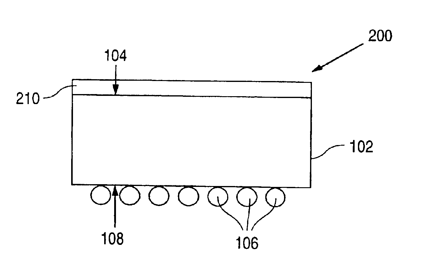
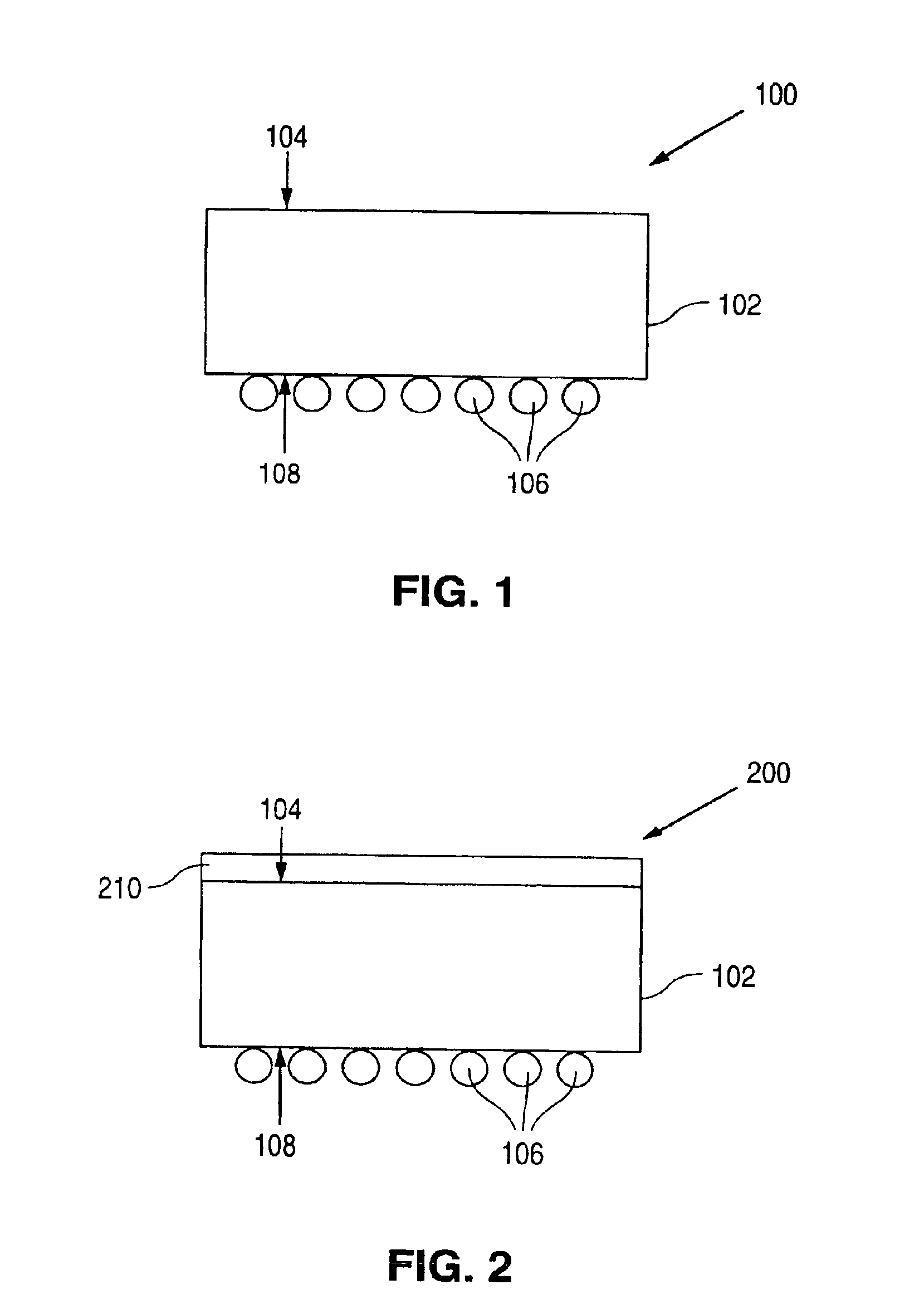
[0020]In general, the present invention includes a wafer having a protective film for substantially preventing damage to the dies of the wafer during and after the dicing process. For example, the protective film substantially prevents chipping along the dicing edges of the dies. Although the following description is in reference to flip chip devices, of course, it should be well understood to those skilled in the art that the present i...


PUM


Abstract

Disclosed is a packaged integrated circuit device. The device includes a die having a plurality of electrical contacts on a first surface of the die and a protective film adhered directly to a back surface of the die, the protective film being thick enough to allow laser marking of the protective film without the laser penetrating to the die. In one preferred embodiment, the protective film of the device is a thick film formed by screen printing. In a preferred embodiment, the protective film has a thickness of between about 1.5 and 5 mils. Also, disclosed is a method of fabricating a semiconductor wafer having a wafer substrate with a top surface and a bottom surface and a plurality of dies. In this embodiment, the method includes providing a plurality of dies on the top surface of the wafer substrate, applying a thick film over the bottom surface of the wafer substrate, adhering the thick film to a mounting tape that is not ultraviolet curable, and dicing the wafer to separate the dies. The thick film reduces chipping along edges of the separated dies.

Description

CROSS REFERENCE TO RELATED APPLICATIONS[0001]This application is related to U.S. patent application Ser. No. 08 / 517,603 filed Aug. 22, 1995 entitled, “Thermally Enhanced Micro-Ball Grid Array Package” by Rajeev Joshi having assignment rights in common with the present invention, which is herein incorporated by reference.BACKGROUND OF THE INVENTION[0002]The present invention relates generally to integrated circuit (IC) devices and, more particularly, to a semiconductor wafer having a bottom surface that is coated with a protective coating prior to the performance of a wafer dicing, or die singulation, operation.[0003]Currently, in order to remain competitive in the IC industry, IC process engineers must continuously increase device yield per wafer or lot. That is, process engineers seek to increase the number of usable semiconductor devices per wafer. Since any step in the fabrication process may detrimentally affect the IC device yield, process engineers seek to optimize each step a...

Claims


Application Information

Patent Timeline
Patent Type & Authority Patents(United States)
IPC IPC(8): H01L23/58H01L21/56H01L23/00H01L23/31H01L23/544
CPCH01L21/56H01L23/3157H01L23/544H01L23/562H01L2223/54473H01L2223/5448H01L2224/16H01L2224/274H01L2924/01068
Inventor KAO, PAI-HSIANGSCHAEFER, WILLIAM JEFFREYKELKAR, NIKHIL VISHWANATH
Owner NAT SEMICON CORP
Why Eureka
Try Eureka