Dual loading port semiconductor processing equipment

Inactive Publication Date: 2011-12-13
KOKUSA ELECTRIC CO LTD
View PDF31 Cites 239 Cited by
  • Summary
  • Abstract
  • Description
  • Claims
  • Application Information

AI Technical Summary

Benefits of technology

[0008]It is, therefore, a primary object of the present invention to provide a

Problems solved by technology

However, since the conventional semiconductor processing equipment is provided with only a single wafer loading port, the lead time required in preparing wafers for an actual process increases due to replacement of a pod on the wafer loading port with another, which in turn lengthens the over

Method used


Image

  • Dual loading port semiconductor processing equipment
  • Dual loading port semiconductor processing equipment
  • Dual loading port semiconductor processing equipment

Examples


first embodiment

[0048]FIG. 7 illustrates the pod transferring process between the pod shelf 12 and the wafer loading ports 13 and also the wafer transferring process between the pods on the wafer loading ports 13 and the wafer boat 8 in accordance with the present invention.

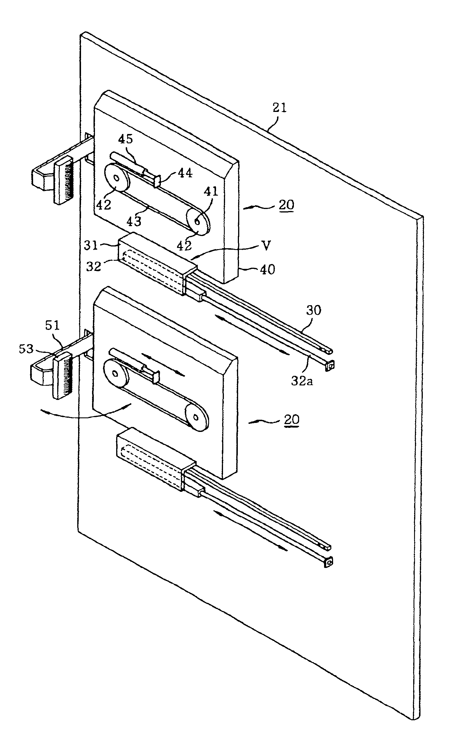
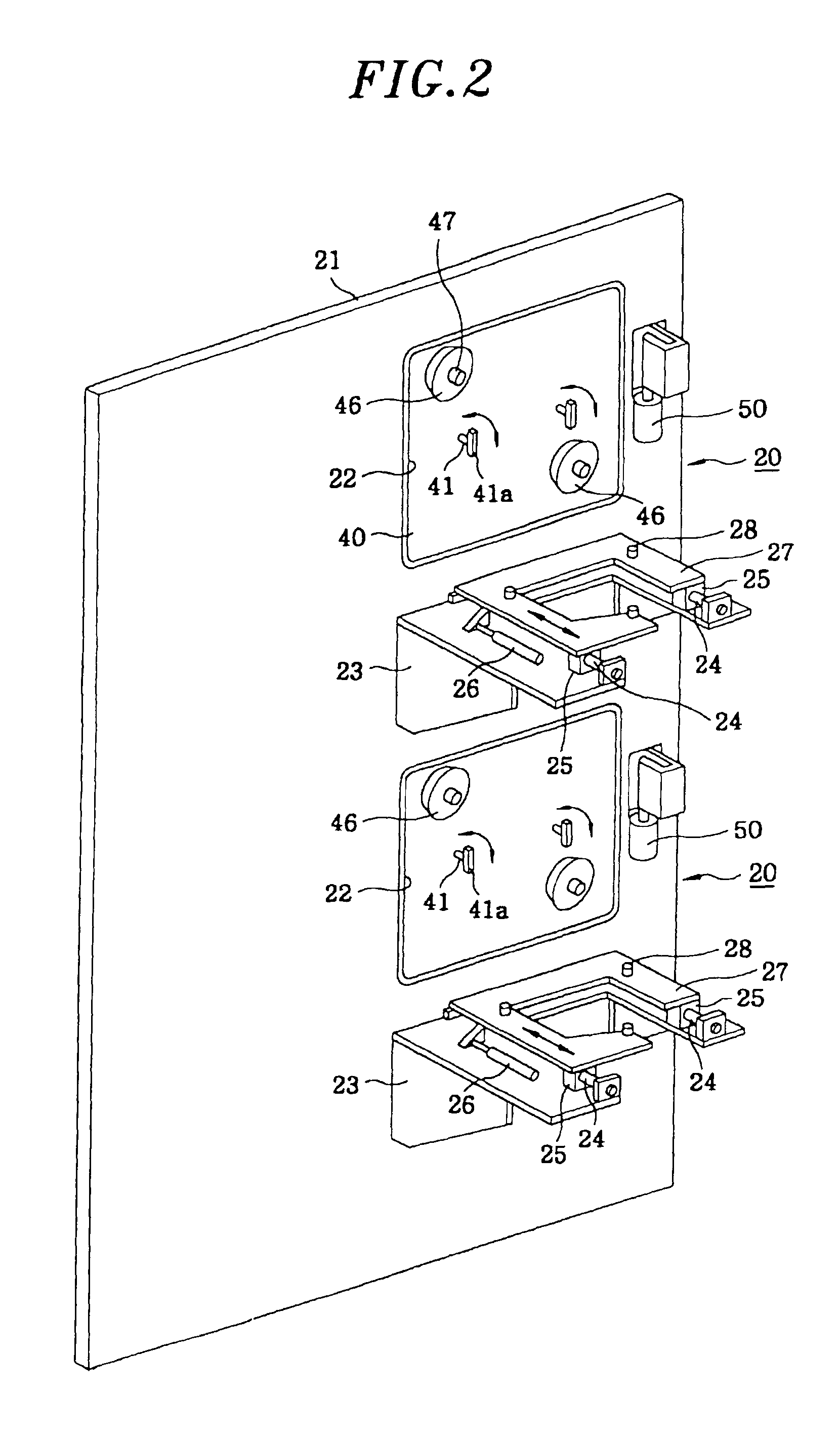
[0049]The two pod openers 20 are arranged to close the openings 22 such that the packing member 55 seals against the rear side wall of the bulkhead 21. One pod 10 is transferred from the pod shelf 12 to, e.g., the upper wafer loading port 13 by the pod handler 14 and disposed on the loading platform 27. The three alignment pins 28 on the loading platform 27 engage with the corresponding three holes (not shown) formed under the pod 10 to thereby complete the alignment of the pod 10 on the loading platform 27.

[0050]The pod 10 provided on the loading platform 27 is moved toward the bulkhead 21 by the extension of the air cylinder 26 in such a manner that the respective packing members 54 and 56 are airtightly in contact with the po...

second embodiment

[0074]The wafer transferring sequence in accordance with the present invention will be described with reference to FIG. 8. At the first stage of the sequence for transferring unprocessed wafers to the wafer boat 8, a first pod containing unprocessed wafers is transferred from the pod shelf 12 to a first wafer loading port (process “A”) and the door of the first pod is opened (process “B”).

[0075]Immediately thereafter at the second stage, wafer transferring from the first pod to the wafer boat 8 (process “D”) starts and, at the same time, a second pod containing the unprocessed wafers are transferred to a second wafer loading port (process “A”) and waits until the wafer transferring process “D” at the first wafer loading port is completed (process “F”).

[0076]At the third stage, the door of the second pod is opened (process “B”) and the wafers therein are transferred to the boat 8 (process “D”) and the door is restored on the empty first pod (process “E”), which is then replaced with ...


PUM


Abstract

A substrate processing equipment comprises two pod supporting stages and two independently operable pod door openers. Each pod supporting stage is capable of placing thereon a pod for containing substrates therein. Each pod door openers having means for permitting access to the substrates inside the pod placed on a corresponding pod supporting stage.

Description

CROSS-REFERENCES TO RELATED APPLICATIONS[0001]The present application claims priority from Japanese Patent Application No. 2000-114818, filed Apr. 17, 2000, and is a reissue application of U.S. Pat. No. 6,641,350, issued Nov. 4, 2003, the contents of which are incorporated herein by reference. More than one reissue application has been filed for the reissue of U.S. Pat. No. 6,641,350. The reissue applications are application Ser. No. 12 / 724,026 (the present application), and application Ser. Nos. 12 / 724,613 and 12 / 724,625, both filed Mar. 16, 2010, and both of which are continuation reissue applications of the present application, and both of which are now abandoned.FIELD OF THE INVENTION[0002]The present invention relates to a semiconductor processing equipment; and, more particularly, to a device for moving doors of substrate carriers, e.g., for use in a semiconductor processing equipment such as a batch-type vertical apparatus for performing a diffusion or a CVD (chemical vapor d...

Claims


Application Information

Patent Timeline
IPC IPC(8): F26B21/06B65G49/07H01L21/677
CPCH01L21/67772H01L21/67775Y10S414/14H01L21/68
Inventor NAKASHIMA, TAKANOBUMATSUNAGA, TATSUHISAYANAGAWA, HIDEHIRO
Owner KOKUSA ELECTRIC CO LTD
Why Eureka
Try Eureka