Leadframe semiconductor integrated circuit device using the same, and method of and process for fabricating the two

a semiconductor integrated circuit and leadframe technology, applied in semiconductor devices, semiconductor/solid-state device details, electrical apparatus, etc., can solve problems such as difficult to prevent effective package body cracking, wire bonding defect, and considerable restriction on the size of the chip to be mounted on the die pad. , to achieve the effect of suppressing package body cracking and widening the size rang

Inactive Publication Date: 2012-06-05
RENESAS ELECTRONICS CORP
View PDF40 Cites 8 Cited by
  • Summary
  • Abstract
  • Description
  • Claims
  • Application Information

AI Technical Summary

Benefits of technology

[0037]More specifically, in case the leadframe of the prior art, i.e., the leadframe in which the external size of the die pad is larger than the chip size is used, the size of the chips to be commonly used is limited to a considerable small range (i.e., 1 to 2 mm from the contour of the tab to the chip end) so that the leading ends of the inner leads need not be cut. On the other hand, the leadframe of the present invention has a smaller die pad than the chip size so that it can commonly use chips o a wider size range (e.g., 5×5 mm to 15×15 mm). Thus, the leadframe of the present invention can sufficiently match the case in which the positions of the leading ends of the inner leads have to be changed according to the limits to the wire length.
[0038]M

Problems solved by technology

Since the resin is made far thinner than that of the prior LSI package, the aforementioned counter-measures, i.e., the method of forming the through holes in the die pad or dimpling the die pad has found it difficult to prevent the package body cracking effectively.
However, these investigations have revealed that a considerable restriction is exerted upon the size of the chip to be mounted on the die pad.
Specifically, if there is mounted a semiconductor chip having an external size smaller by 1 to 2 mm or more than that of the die pad, the wires will hang as far as to

Method used


Image

  • Leadframe semiconductor integrated circuit device using the same, and method of and process for fabricating the two
  • Leadframe semiconductor integrated circuit device using the same, and method of and process for fabricating the two
  • Leadframe semiconductor integrated circuit device using the same, and method of and process for fabricating the two

Examples


Embodiment Construction

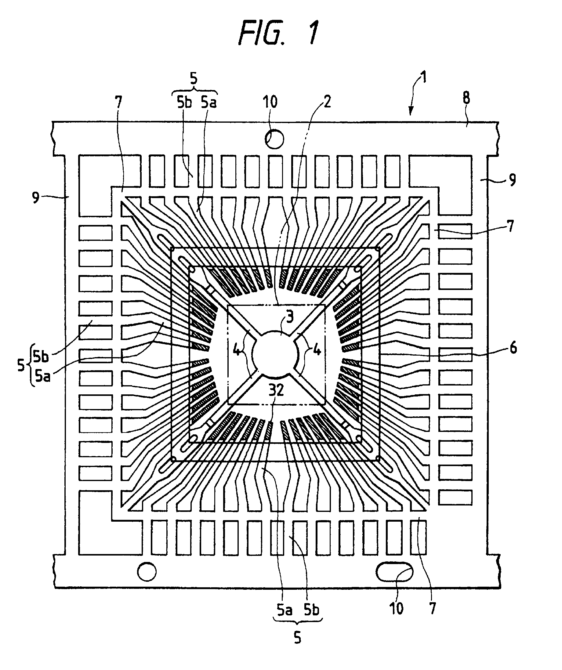
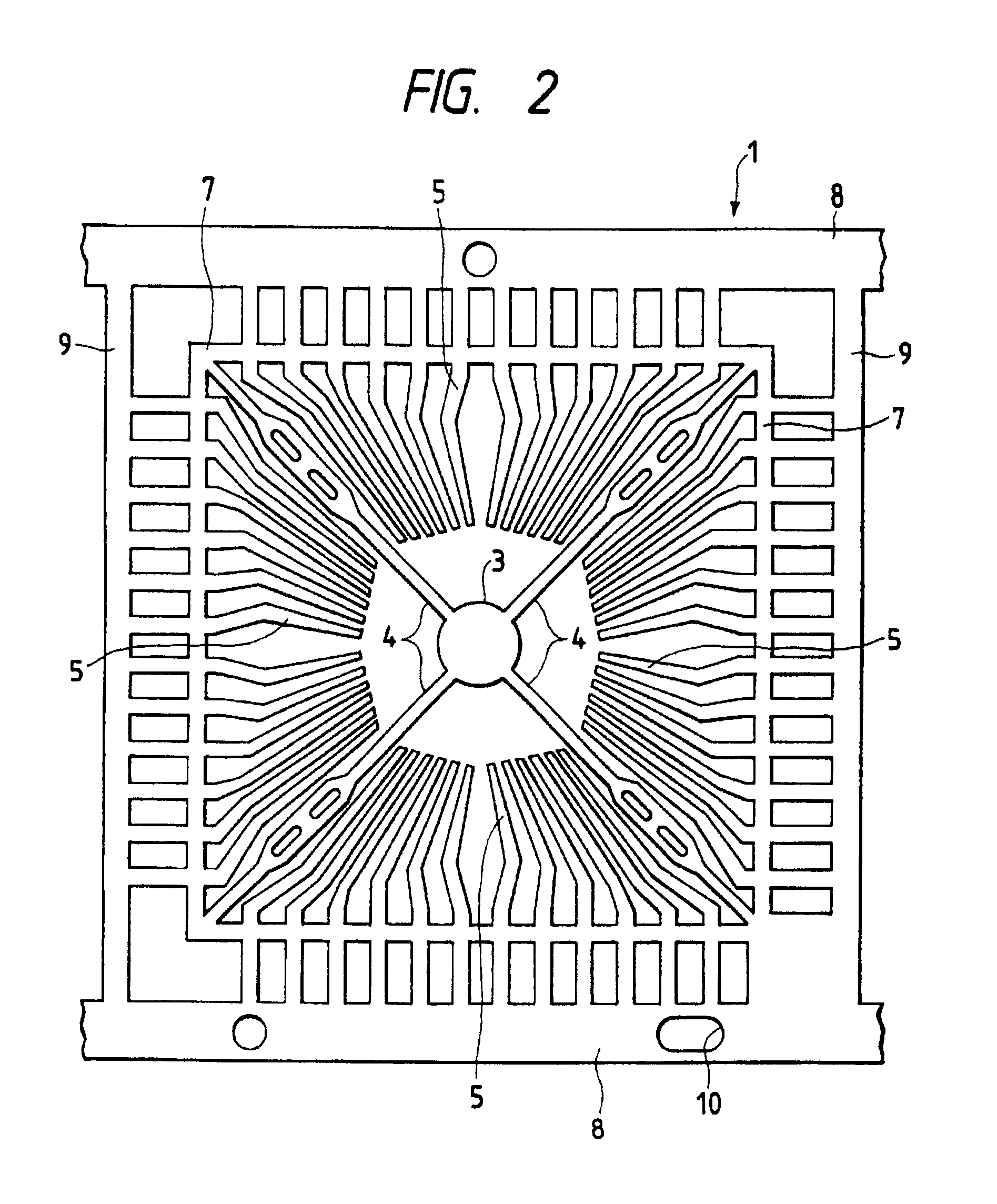
[0072]FIG. 1 is a top plan view showing a leadframe to be used for fabricating a QFP package according to one embodiment of the present invention.

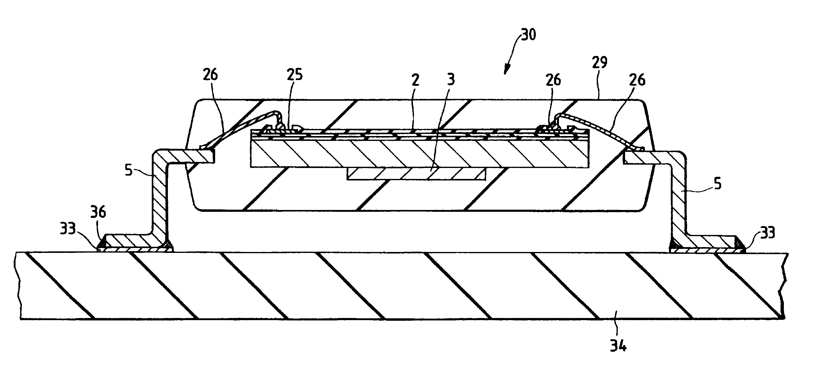
[0073]A leadframe 1 is formed at its central portion with a circular die pad for mounting a semiconductor chip 2 which is formed with a semiconductor circuit and bonding pads on its principal face. The die pad 3 is supported by four suspension leads 4. The die pad 3 has its chip mounting face characterized to have a smaller area than that of the principal face of the semiconductor chip 2 mounted thereon.

[0074]The die pad 3 is arranged therearound with a plurality of leads 5. To the wider portions of the suspension leads 4 and the middle portions of the leads 5, there is adhered a quadrangular frame-shaped tape 6 which is made of an insulating, thin synthetic resin film. Outside of the tape 6, there is formed a dam bar 7 for supporting the leads 5 and preventing the resin from overflowing at a molding time. The dam bar 7 is formed into a fr...


PUM

PropertyMeasurementUnit
Volumeaaaaaaaaaa
Volumeaaaaaaaaaa
Volumeaaaaaaaaaa

Abstract

In order to improve the package body cracking resistance of an LSI package at the reflow soldering and to provide both a leadframe suitable for fabricating the LSI package according to the flexible manufacturing system and an LSI using the leadframe, the adhered area between a semiconductor chip 2 and a resin is enlarged by making the external size of a die pad 3 smaller than that of the semiconductor chip to be mounted thereon. Moreover, a variety of semiconductor chips 2 having different external sizes can be mounted on the die pad 3 by cutting the leading ends of leads 5 to a suitable length in accordance with the external sizes of the semiconductor chips 2.

Description

[0001]This application is a 37 CFR §1.60 divisional of prior application Ser. No. 08 / 038,684, filed Mar. 29, 1993 (allowed).Notice: More than one reissue application has been filed for the reissue of U.S. Pat. No. 5,637,913 now abandoned. The reissue cases are application Ser. No. 09 / 328,910 filed 9 Jun. 1999, pending, and its divisions, application Ser. No. 09 / 987,978 filed 16 Nov. 2001 (the present case), pending, and application Ser. No. 09 / 989,242 filed 21 Nov. 2001, pending. U.S. application Ser. No. 08 / 311,021 filed on Sep. 22, 1994, now U.S. Pat. No. 5,637,913, issued on Jun. 10, 1997 is a 35 USC §120 Divisional of prior application Ser. No. 08 / 038,684, filed Mar. 29, 1993, now U.S. Pat. No. 5,378,656, issued on Jan. 3, 1995. This application Ser. No. 09 / 987,978, filed Nov. 16, 2001, is a divisional application of Ser. No. 09 / 328,910, filed Jun. 9, 1999.BACKGROUND OF THE INVENTION[0002]The present invention relates to a leadframe for mounting a semiconductor chip, a semicondu...

Claims


Application Information

Patent Timeline
IPC IPC(8): H01L23/495H01L23/50H01L21/48H01L21/52H01L21/60
CPCH01L21/4842H01L23/49503H01L23/49513H01L23/49541H01L24/27H01L24/83H01L24/32H01L24/29H01L24/743H01L2224/29007H01L2224/32014H01L2224/32245H01L2224/48091H01L2224/48247H01L2224/48465H01L2224/49171H01L2224/73265H01L2224/83194H01L2224/838H01L2224/92247H01L2924/01004H01L2924/01005H01L2924/01029H01L2924/01047H01L2924/01078H01L2924/01079H01L2924/01082H01L2924/14H01L2924/1433H01L24/48H01L2224/2919H01L2924/01006H01L2924/01023H01L2924/01033H01L2924/014H01L2924/0665H01L24/45H01L2224/02166H01L2224/45144H01L2224/743H01L2224/82181H01L2224/83192H01L2224/85181H01L2224/92H01L2924/01014H01L24/49Y10T29/49121H01L2224/859H01L2924/00014H01L2924/00012H01L2924/00H01L2924/3512H01L2924/181H01L24/73H01L2224/32055H01L2224/05599H01L23/495
Inventor KAJIHARA, YUJIROSUZUKI, KAZUNARITSUBOSAKI, KUNIHIROSUZUKI, HIROMICHIMIYAKI, YOSHINORINAITO, TAKAHIROKAWAI, SUEO
Owner RENESAS ELECTRONICS CORP
Why Eureka
Try Eureka