Back-flow pulling face down welding method of infrared focus planar detector

A technology of infrared focal plane and welding method, applied in semiconductor/solid-state device manufacturing, electrical components, circuits, etc., can solve problems such as inability to achieve precise control of In bumps, improve mechanical and electrical properties, and reduce extrusion. strength, the effect of improving wettability

Inactive Publication Date: 2007-12-12
SHANGHAI INST OF TECHNICAL PHYSICS - CHINESE ACAD OF SCI
View PDF3 Cites 0 Cited by
  • Summary
  • Abstract
  • Description
  • Claims
  • Application Information

AI Technical Summary

Problems solved by technology

The advantage of this method is that the extrusion force is small, and it only needs to prepare In bumps on one side and welding pads on the other side; however, it cannot achieve precise control of the shape and height of In bumps, and the photosensitive array The chip also needs to undergo high-temperature reflow treatment at the melting point of In

Method used


Image

  • Back-flow pulling face down welding method of infrared focus planar detector
  • Back-flow pulling face down welding method of infrared focus planar detector
  • Back-flow pulling face down welding method of infrared focus planar detector

Examples


Embodiment Construction

[0022] Taking a preferred embodiment as an example below, the specific implementation manner of the present invention is described in further detail:

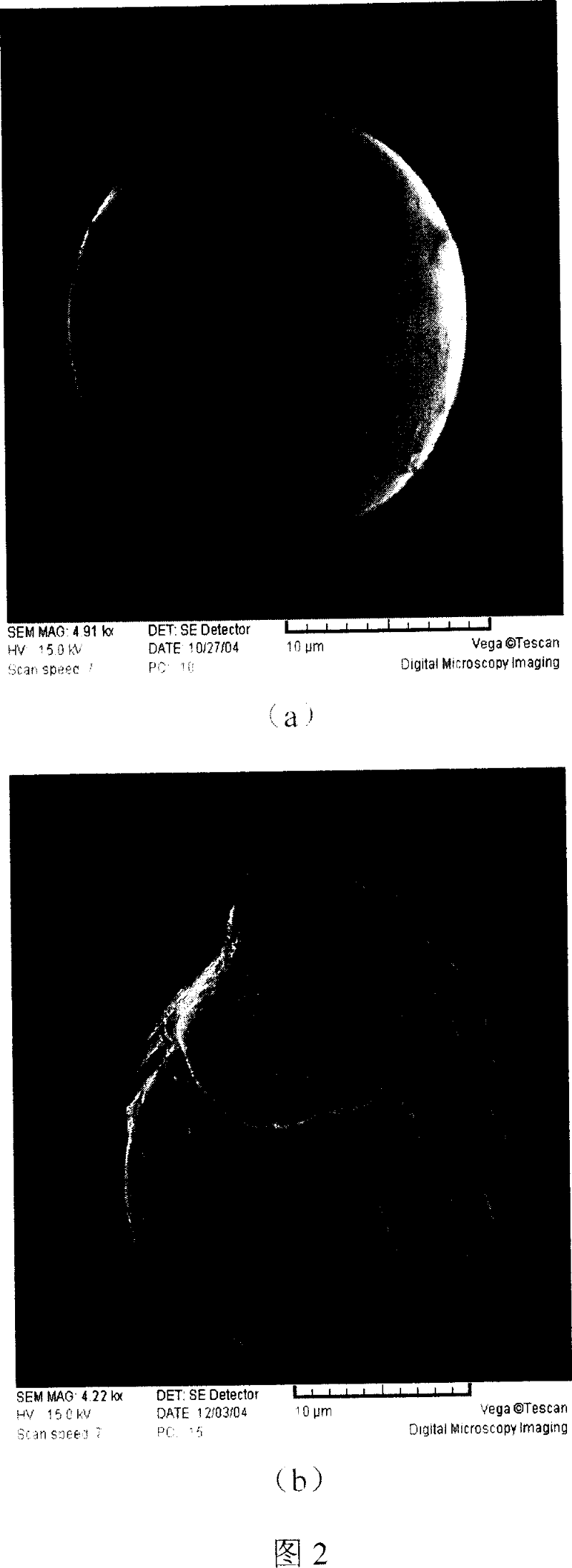
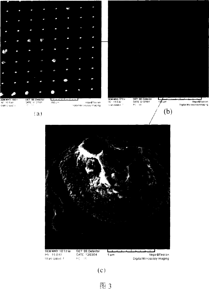
[0023] Flip-chip soldering sample of the present invention: the area of ​​the silicon readout circuit is 6×9mm 2 , a total of 2040 In ball arrays, and the area of ​​the HgCdTe photosensitive array chip on the GaAs substrate is 4×6mm 2 , also prepared 2040 Cr / Au soldering pad arrays. Among them, the height of the In bump is 16.5 μm, the diameter is 19.5 μm, and the diameters of the welding pressure point and the In bump are both 14 μm.

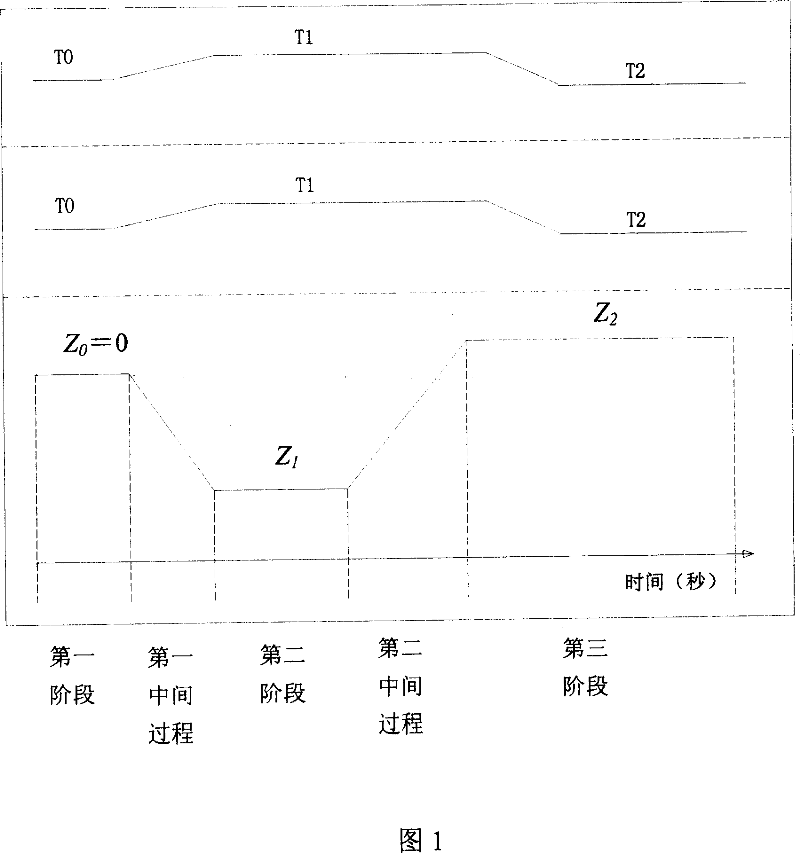
[0024] Install the above-prepared In ball array silicon readout circuit and the array chip with soldering pads on the French SUSS company model FC150 flip-chip welding equipment, and perform single-sided In ball reflow pull-up welding, as shown in Figure 1 :

[0025] A. The first stage: the silicon readout circuit and the array chip start to contact and maintain the contact state.

[0026] F...


PUM


Abstract

This invention discloses a back-flow pulling flip-chip method of an infrared focal plane detector characterizing in preparing an In ball array on a Si read-out circuit, preparing welding pressing points and applying a single edge In ball back-flow vibration pulling flip-chip method, which is advantaged at avoiding the bad influence on the performance brought with the high temperature back flow endured by In melting point processed to an infrared photosensitive array chip by this invented method and generating tiny swing come-and go movement between the welding pressing points and the In ball of the read-out circuit to rub the oxidation layer of the In ball surface to increase the moist of the In ball at the back-flow state and the welding pressing points.

Description

technical field [0001] The invention relates to a preparation process of an infrared focal plane detector, in particular to a reflow pulling flip-chip welding method between a photosensitive array chip of the focal plane detector and a silicon readout circuit. Background technique [0002] The infrared focal plane detector is composed of an infrared photosensitive array chip and its corresponding silicon readout circuit, both of which are connected based on the flip-chip welding technology of metal indium (In) bumps. [0003] At present, there are two commonly used flip chip welding methods for infrared focal plane detectors: one is the flip chip cold pressure welding method, which is carried out on the alignment welding equipment. The array chip is aligned with the silicon readout circuit, which also has an array of In bumps, and then some pressure is applied to solder them together. Although this method is simple and practical, it has disadvantages such as large extrusion...

Claims


Application Information

Patent Timeline
Patent Type & Authority Patents(China)
IPC IPC(8): H01L21/607H01L21/60
Inventor 叶振华胡晓宁王建新何力
Owner SHANGHAI INST OF TECHNICAL PHYSICS - CHINESE ACAD OF SCI
Why Eureka
Try Eureka