
Solid camera device and camera using same

A device and sensor technology, applied in the field of solid-state imaging devices for AEAF, can solve the problems of difficulty in adopting small cameras, high price and large size of cameras, etc.

Inactive Publication Date: 2008-02-20
CANON KK
View PDF4 Cites 0 Cited by
  • Summary
  • Abstract
  • Description
  • Claims
  • Application Information

AI Technical Summary

Problems solved by technology

This causes high price and large size of the camera, so it is difficult to adopt for small cameras

Method used


Image

  • Solid camera device and camera using same
  • Solid camera device and camera using same
  • Solid camera device and camera using same

Examples


Embodiment 1

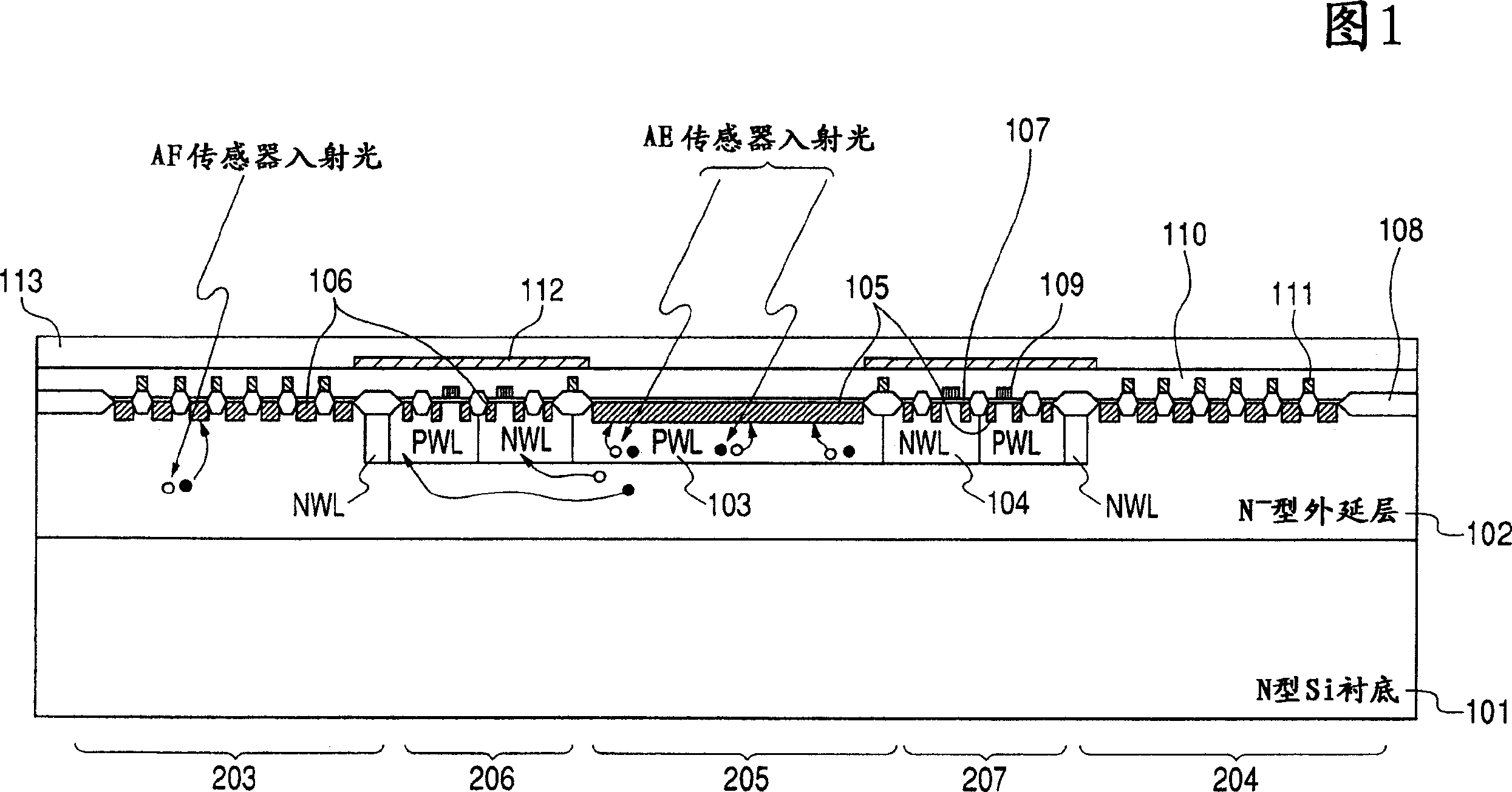
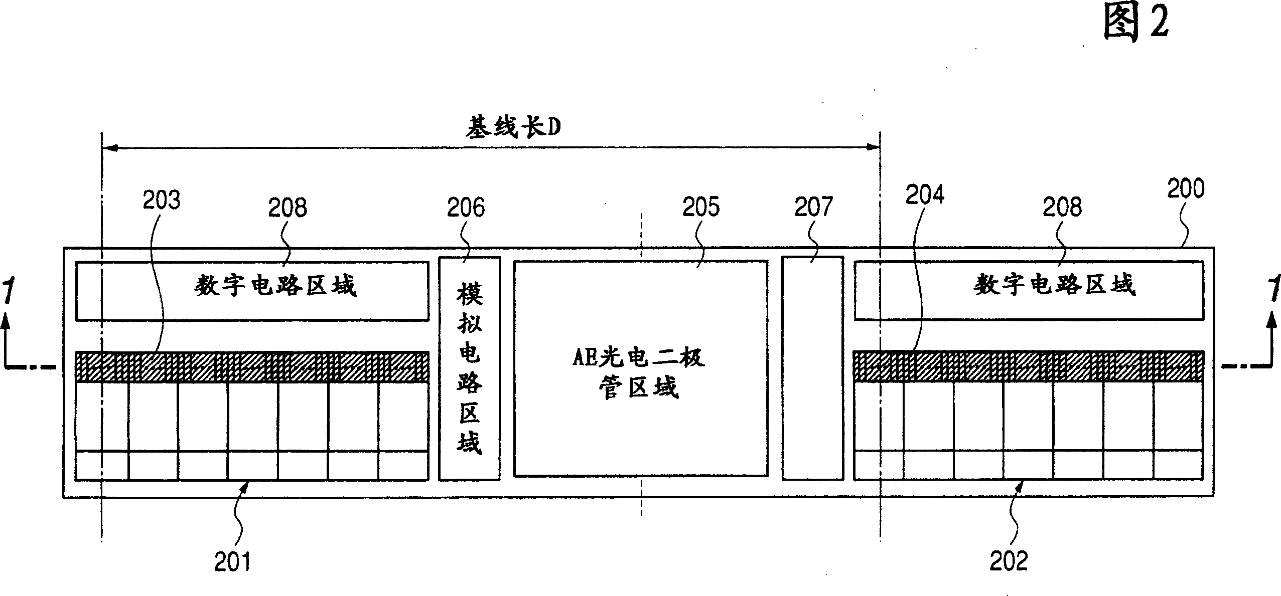
[0024] FIG. 1 is a view most fully showing the features of the present invention, and is a schematic sectional structural view of the solid-state imaging device of the present invention. In addition, FIG. 2 shows a schematic plan layout of the solid-state imaging device of the present invention. Fig. 1 is a sectional view of part 1-1 of Fig. 2 . This example uses N - A solid-state imaging device manufactured by a double-well structure CMOS process of a P-type well (PWL) and an N-type well (NWL) of an epitaxial wafer.

[0025] In Fig. 1, 101 is an N-type Si substrate, and 102 is an N-type Si substrate. - Type epitaxial layer, 103 is P-type well (PWL), 104 is N-type well (NWL), 105 is N + Type impurity diffusion region (NSD), 106 is P + Type impurity diffusion region (PSD), 107 is a gate oxide film, 108 is a thick selective oxide film as an element isolation region, 109 is a POL (polysilicon) wiring that also serves as a gate of a MOS transistor, 110 is an interlayer insulat...

Embodiment 2

[0032] Fig. 4 is a cross-sectional view showing a solid-state imaging device embodying a second embodiment of the present invention. In this figure, 210 is N + Type impurity buried layer (NBL). For this embodiment, compared with the first embodiment, the N-type Si substrate 101 and N - The NBL 210 is provided between the epitaxial layers 102, and the potential barrier generated by the NBL can prevent the diffusion current from inside the Si substrate 101 from flowing into the photodiode of the AF sensor. In particular, since the photodiode for the AF sensor is formed in the epitaxial layer, the diffusion current of the Si substrate 101 has a great influence, and this embodiment will be very effective. Moreover, the method of internal degassing treatment is adopted in the process, which can further reduce the dark current.

[0033] In this embodiment, by reducing the dark current generated by the photodiode for the AF sensor, a solid-state imaging device for AEAF that improv...

Embodiment 3

[0035] Fig. 5 is a sectional structural view of a solid-state imaging device according to a third embodiment of the present invention. In this figure, 300 is a low-concentration P-type well. In the first and second embodiments, the photodiode for the AF sensor is provided in the epitaxial layer, but in the present embodiment, the impurity concentration is low, and it is provided in the deep PWL 300 of the junction depth. The usual PWL103 has a surface concentration of 1×10 17 cm -3 About, for the junction depth below 1μm, the deep PWL300 should be formed in this way, using high-energy ion implantation equipment, so that the impurity concentration near the surface is about 1×10 16 cm -3 , PWL junction depth is more than 2μm. Therefore, the AF sensor is also formed in the PWL similarly to the AE sensor, so that an epitaxial layer is basically not required.

[0036] In this embodiment, the depletion layer of the photodiode for AF is extended to the PWL side by reducing the i...


PUM


Abstract

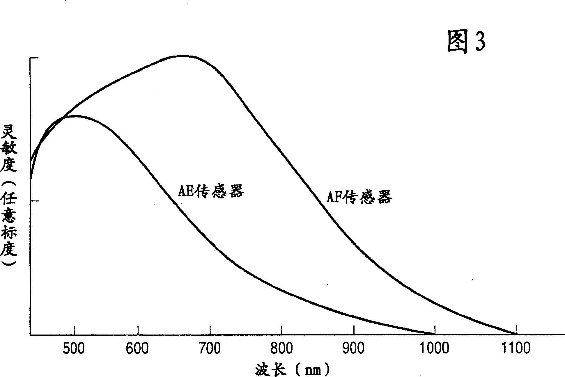
An AE / AF solid-state imaging apparatus exhibiting suitable characteristics of spectral sensitivities of an AE sensor and an AF sensor respectively, wherein visual sensitivity corrections filters of an optical system are reduced. The solid-state imaging apparatus includes AF photodiode regions (203, 204) for auto-focusing and an AE photodiode region (205) for executing a photometric process of a photographing region, integrated on a common semiconductor substrate (101). The characteristics of spectral sensitivities of the AF photodiode regions (203, 204) are different from the characteristic of the spectral sensitivity of the AE photodiode region (205). Desirably, a peak wavelength of each of the spectral sensitivity characteristics of the AF photodiode regions is positioned on a longer wavelength side than a peak wavelength of the AE photodiode region.

Description

technical field [0001] The present invention relates to a solid-state imaging device for AEAF, in particular, a passive type solid-state imaging device for AEAF suitable for use in a lens-shutter compact camera. [0002] Furthermore, the present invention relates to a video camera using the aforementioned solid-state imaging device for AEAF. Background technique [0003] Conventionally, there is a solid-state imaging device for photometry and distance measurement disclosed in US Pat. FIG. 7 shows a schematic plan layout of the solid-state imaging device. In the figure, 30 is a sensor array for photometry, 32 is a center segment for photometry, 34A to 34D are inner segments for photometry (AE), 36A to 36D are outer segments for photometry, 40 and 42 are A sensor array for ranging (AF), 44l-n and 46l-n are pixels, 50 is a Si semiconductor substrate, H and W are the size of the photometry area, and D is the base line length. [0004] Since this sensor performs distance measu...

Claims


Application Information

Patent Timeline
Patent Type & Authority Patents(China)
IPC IPC(8): H01L27/146H04N5/335H04N5/225G01J1/02G02B7/28G03B7/099H01L27/14H01L27/144H01L31/10H04N23/75H04N25/00
CPCH01L27/144Y02E10/547
Inventor 高橋秀和
Owner CANON KK
Learn More