Germanium-silicon schottky diode and its production method

A Schottky diode, germanium-silicon technology, applied in semiconductor/solid-state device manufacturing, electrical components, circuits, etc., can solve the problems of device isolation and integration process limitations, and achieve the goal of reducing interface density, improving integration, and simplifying processes. Effect

Inactive Publication Date: 2008-02-27
ZHEJIANG UNIV
View PDF5 Cites 5 Cited by
  • Summary
  • Abstract
  • Description
  • Claims
  • Application Information

AI Technical Summary

Problems solved by technology

Since silicon germanium materials will undergo strain relaxation at high temperatures, only low-temperature deposition of silicon nitride is used, which brings great limitations to the subsequent device isolation and integration processes.

Method used


Image

  • Germanium-silicon schottky diode and its production method

Examples


Embodiment Construction

[0018] The present invention is further described below in conjunction with specific examples.

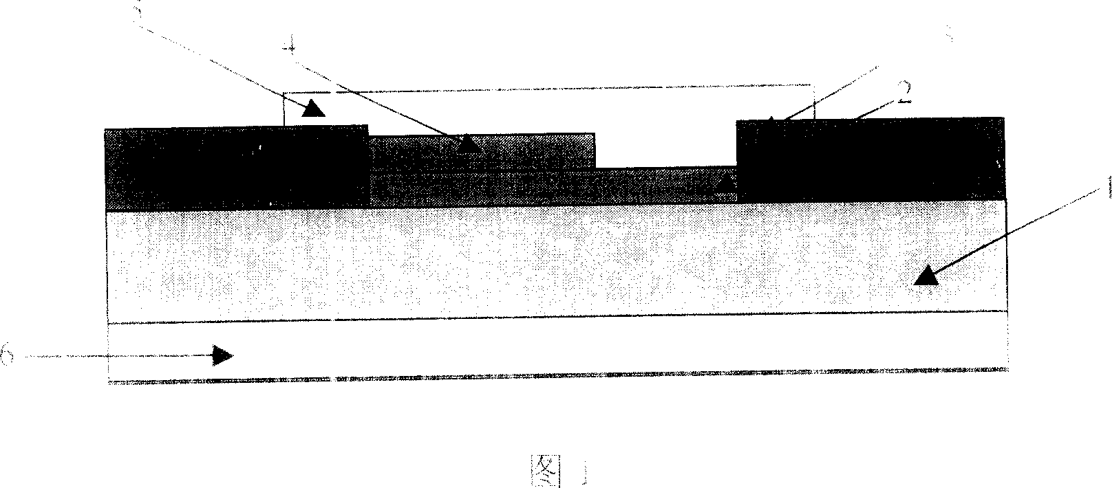
[0019] Referring to Fig. 1, the SiGe Schottky diode of the present invention comprises a silicon substrate 1, a silicon germanium layer 2, a silicon nitride layer 3 with a window, a nickel-silicon compound layer 4, an aluminum electrode 5 and an ohmic contact electrode 6, the ohmic The contact electrode 6, the silicon substrate 1 and the silicon nitride layer 3 with a window are successively stacked from bottom to top, and the silicon germanium layer 2 and the nickel-silicon compound layer 4 are in the window of the silicon nitride layer 3, wherein the nickel-silicon compound layer Layer 4 is on top of silicon germanium layer 2, covering the aluminum electrodes in contact with the nickel silicon compound layer over the windows of the silicon nitride layer.

[0020] The manufacturing method of silicon germanium Schottky diode, the steps are as follows:

[0021] 1) Clean the N-type ...


PUM

PropertyMeasurementUnit
thicknessaaaaaaaaaa
thicknessaaaaaaaaaa
electrical resistivityaaaaaaaaaa

Abstract

The Schottky diode consists of: ohmic contact electrode stacked in sequence from bottom to top; silicon substrate and silicon nitride layer on which a window is opened, in the window there are germanium silicon layer and nisiloy layer. The nisiloy layer is above the germanium silicon layer. The aluminium electrode touching the nisiloy compound covers the window of silicon nitride. The making method includes following steps: first a silicon layer is developed on the silicon substrate; deposits a silicon dioxide layer on silicon nitride and photoetches a window; develops germanium silicon layer; with dilute hydrofluoric acid, strips silicon dioxide layer; metallic nickel is coated by vaporization on germanium silicon layer; anneal to form germanium silicon compound layer; coats by vaporization aluminium electrode and ohmic contact electrode.

Description

technical field [0001] The invention relates to a semiconductor device, in particular to a germanium-silicon Schottky diode and a manufacturing method thereof. Background technique [0002] Schottky diodes are widely used in high-frequency, high-speed, and detection due to their characteristics of majority carrier operation, fast response speed, and no minority carrier accumulation. Before the present invention was made, the traditional SiGe Schottky diodes had an ohmic contact electrode, a silicon substrate layer, a SiGe epitaxial layer, and a silicon nitride layer with a window from bottom to top. There is a nickel-silicon compound layer, and the silicon nitride window is covered with an aluminum electrode. The silicon germanium Schottky diode with this structure has a large contact area between the silicon germanium and the silicon nitride, and there are many interface defects, resulting in a large leakage current of the device. During the manufacturing process, a silico...

Claims


Application Information

Patent Timeline
Patent Type & Authority Patents(China)
IPC IPC(8): H01L29/872H01L21/329
Inventor 叶志镇吴贵斌唐九耀赵星刘国军
Owner ZHEJIANG UNIV
Why Eureka
Try Eureka