Particle-removing process before semiconductor etching
A semiconductor and process technology, applied in the field of pretreatment of semiconductor etching process, can solve problems such as difficulty in ensuring particle control effect and inability to clean silicon wafers
- Summary
- Abstract
- Description
- Claims
- Application Information
AI Technical Summary
Problems solved by technology
Method used
Image

Examples
Embodiment 1
[0023] In the polysilicon wafer etching process, the equipment used is the PM2 of the Equipment Technology Research Center of the North Microelectronics Base. The structure of the polysilicon wafer used is: 100 Ȧ of silicon dioxide, 3050 Ȧ of polysilicon, and a silicon wafer (substrate substrate).
[0024] The etching process is mainly divided into the following steps:
[0025] 1. Send the silicon wafer to the surface of the electrostatic chuck in the chamber;
[0026] 2. Apply the electrostatic chuck voltage, and fix the silicon wafer on the surface of the electrostatic chuck through electrostatic attraction;
[0027] 3. Through the process gas;
[0028] 4. The pendulum valve adjusts the pressure to the set value;
[0029] 5. Add the lower electrode to start the glow;
[0030] 6. The etching process starts. The etching process mainly includes the following steps:
[0031] 1) BT (Break through), that is, the removal of the natural oxide layer, the process parameters are: ...
Embodiment 2
[0038] According to the method described in embodiment 1, difference is, the process that silicon chip is carried out pretreatment before BT step:
[0039] (1) The chamber pressure is 8mT, the upper electrode power is 400w, and the carrier gas is N 2 60sccm, Cl 2 10 sccm, SF 6 20 sccm, O 2 10sccm, the total gas flow rate is 100sccm, and the time is 5s.
[0040] (2) The chamber pressure is 1mT, the upper electrode power is 400w, and the carrier gas is He30sccm, N 2 20sccm, the time is 10s.
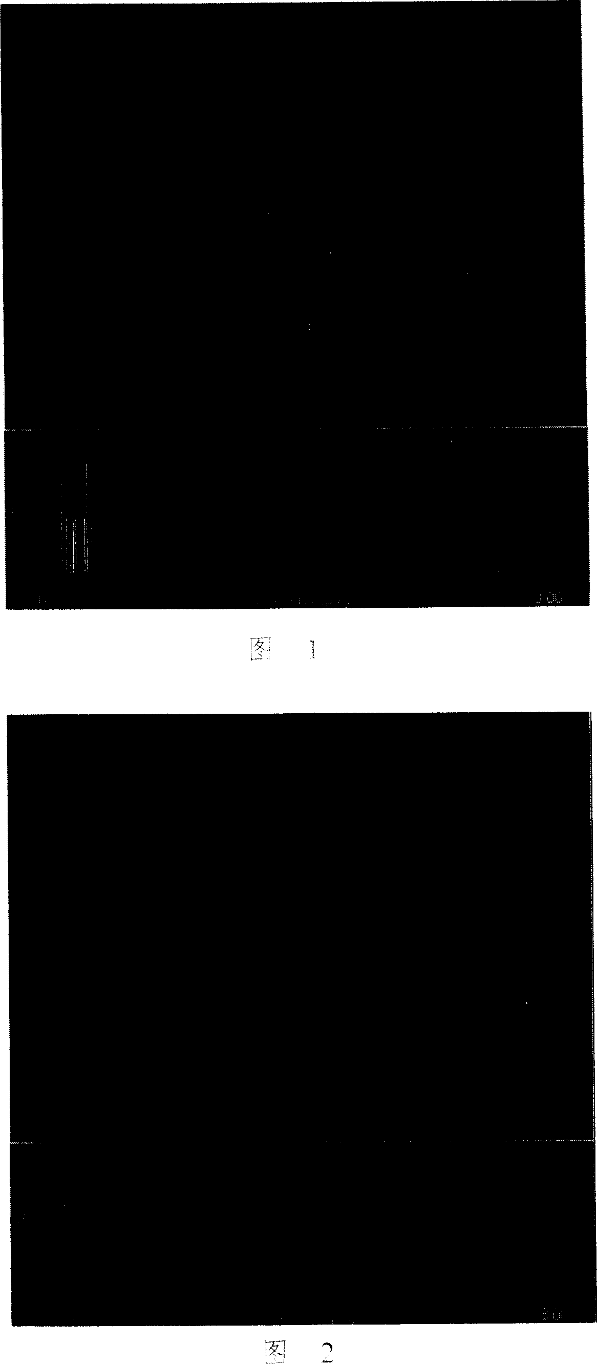
[0041]After the above process, the detection standard is that the number of particles with a size of 0.2um-3um is less than 25 (200mm wafer etch). It is observed by Surfscan 6420 Unpatterned WaferInspection of KLA Company, as shown in Figure 2, it can be seen that the number of particles on the wafer is Particle distribution, the lower part of the figure is the particle size distribution range, specifically, 8 particles with a particle size of 0.2um-3um are obtained.
Embodiment 3
[0043] According to the method described in embodiment 1, difference is, the process that silicon chip is carried out pretreatment before BT step:
[0044] (1) The chamber pressure is 20mT, the upper electrode power is 200w, and the carrier gas is N 2 100sccm, SF 6 40sccm, the time is 25s.
[0045] (2) The chamber pressure is 0.1mT, the upper electrode power is 500w, and the carrier gas is He10sccm, Ar40sccm, N 2 10sccm, the time is 30s.
[0046] After the above process, the detection standard is that the number of particles with a size of 0.2um-3um is less than 25 (200mm wafer etch). Through the detection of Surfscan 6420 Unpatterned WaferInspection of KLA Company, we get the particles with a particle size of 0.2um-3um as 10 pieces.
PUM
 Abstract
Description
Claims
Application Information
 - R&D
- Intellectual Property
- Life Sciences
- Materials
- Tech Scout
- Unparalleled Data Quality
- Higher Quality Content
- 60% Fewer Hallucinations
Browse by: Latest US Patents, China's latest patents, Technical Efficacy Thesaurus, Application Domain, Technology Topic, Popular Technical Reports.
© 2025 PatSnap. All rights reserved.Legal|Privacy policy|Modern Slavery Act Transparency Statement|Sitemap|About US| Contact US: help@patsnap.com