
Method for making metal-oxide-semiconductor transistor

A transistor area, MOS transistor technology, applied in semiconductor/solid-state device manufacturing, electrical components, circuits, etc., to achieve the effect of improving the carrier drift rate

Active Publication Date: 2008-06-04
UNITED MICROELECTRONICS CORP
View PDF4 Cites 0 Cited by
  • Summary
  • Abstract
  • Description
  • Claims
  • Application Information

AI Technical Summary

Problems solved by technology

[0005] Therefore, the main purpose of the present invention is to provide a method for making MOS transistors to solve the insurmountable problems of the prior art

Method used


Image

  • Method for making metal-oxide-semiconductor transistor
  • Method for making metal-oxide-semiconductor transistor
  • Method for making metal-oxide-semiconductor transistor

Examples


Embodiment Construction

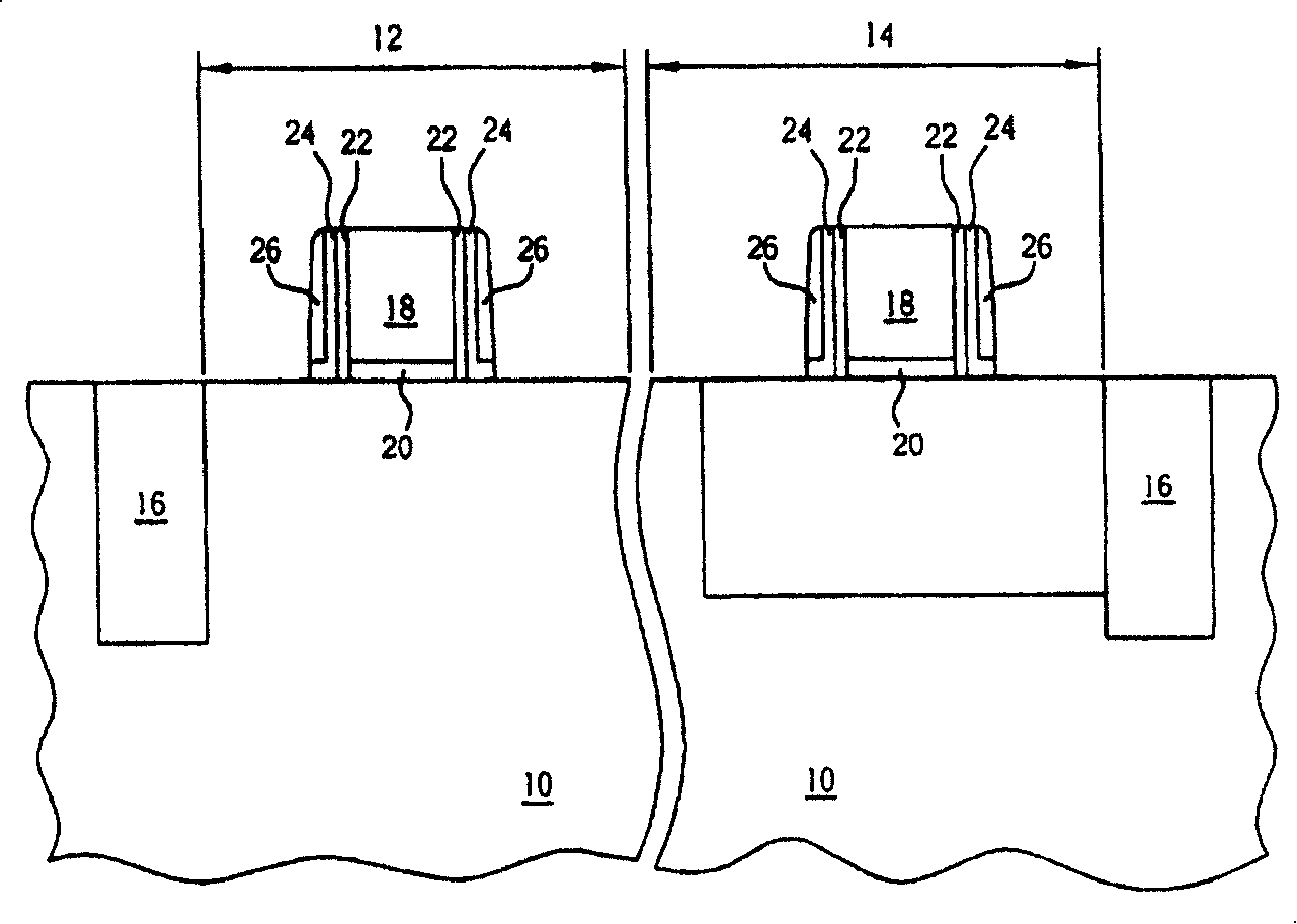
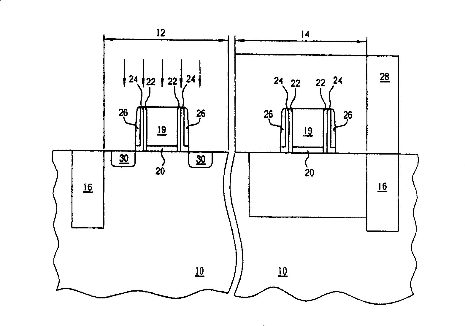
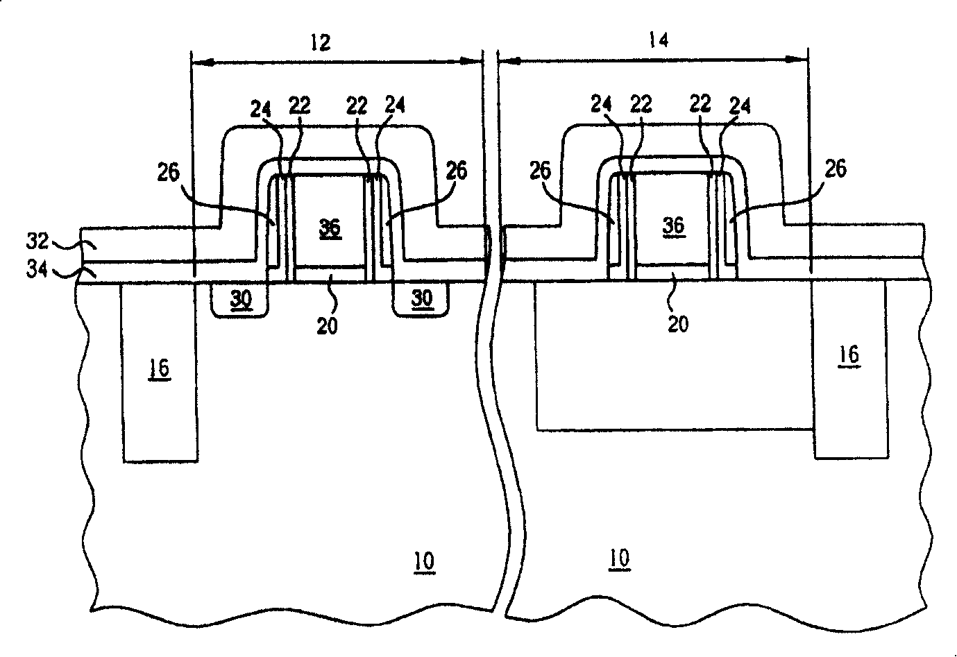
[0029] Please refer to Figure 1 to Figure 5 , Figure 1 to Figure 5 It is a schematic diagram of a method for making a MOS transistor in the first preferred embodiment of the present invention, wherein in order to highlight the characteristics of the present invention and simplify the description, Figure 1 to Figure 5 Only one NMOS transistor region and one PMOS transistor region are shown. Such as figure 1 As shown, a substrate 10, such as a silicon substrate, is provided first. The substrate 10 includes a plurality of NMOS transistor regions 12 and a plurality of PMOS transistor regions 14 separated by shallow trenches 16 . In addition, the substrate 10 further includes a plurality of polysilicon gate structures 18 respectively disposed in each NMOS transistor region 12 and each PMOS transistor region 14 , and a gate insulating layer 20 is further included between each polysilicon gate structure 18 and the substrate 10 . Next, a liner layer 22 , a dielectric layer 24 and...


PUM


Abstract

The disclosed processing method for MOS transistor comprises: providing a substrate with multiple NMOS / PMOS transistor areas and corresponding grid structures arranged between NMOS and PMOS areas; forming a high-tensile thin film on the substrate to cover surfaces of all grid structures; then, taking annealing technique; finally, removing the film.

Description

technical field [0001] The present invention relates to a method for making a MOS transistor, in particular to a method for changing the band structure of a channel region of a substrate by using a high-tension thin film, thereby improving the carrier mobility of the MOS transistor. Background technique [0002] With the continuous shrinking of the line width of the semiconductor process, the size of the MOS (metal-oxide-semiconductor) transistor is also continuously developing towards miniaturization. However, when the line width of the semiconductor process has developed to the bottleneck, how to increase the current carrying capacity Sub-mobility to increase the speed of MOS transistors has become a major topic in the field of semiconductor technology. In the currently known technology, there are MOS transistors using strained silicon as a substrate, which utilizes the characteristic that the lattice constant of the silicon germanium layer is different from that of silico...

Claims


Application Information

Patent Timeline
Patent Type & Authority Patents(China)
IPC IPC(8): H01L21/336H01L21/8234
Inventor 刘毅成陈文吉张子云蓝邦强黄正同萧维沧廖宽仰
Owner UNITED MICROELECTRONICS CORP
Learn More