Germanium-based silicon germanium reduced-field layer LDMOS device structure

A technology of device structure and field drop layer, applied in the field of microelectronics, to achieve the effects of improving radio frequency characteristics, reducing dependence and increasing drift rate

Active Publication Date: 2016-10-26
DONGGUAN SOUTH CHINA DESIGN INNOVATION INST +1
View PDF4 Cites 1 Cited by
  • Summary
  • Abstract
  • Description
  • Claims
  • Application Information

AI Technical Summary

Problems solved by technology

However, the RF performance and withstand voltage capability of silicon-based LDMOSFET devices still need to be further improved

Method used


Image

  • Germanium-based silicon germanium reduced-field layer LDMOS device structure

Examples


Embodiment Construction

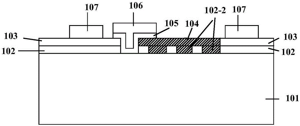
[0022] Combine below figure 1 The present invention will be described in detail.

[0023] A germanium-based silicon germanium field-dropping layer LDMOS device structure proposed in this embodiment, its structure is as follows

[0024] A p-type germanium channel layer (101);

[0025] An N-type doped germanium drift layer (102);

[0026] A heavily N-type doped germanium ohmic contact layer (103);

[0027] A growth layer separated by silicon germanium and germanium as a drift layer (102-2);

[0028] A p-type doped silicon germanium drift field layer (104);

[0029] A gate groove structure whose depth reaches the P-type germanium channel layer;

[0030] an oxide dielectric layer (105) formed in the gate groove;

[0031] a gate metal layer (106) formed in the gate groove;

[0032] A source-drain metal electrode (107) formed in the source-drain region.

[0033] In this embodiment, the drift layer of the LDMOSFET device is made of an epitaxial layer material in which silicon...


PUM


Abstract

The invention discloses a germanium-based silicon germanium reduced-field layer LDMOS device structure which comprises a P-type germanium channel layer, an N-type doped germanium drift layer, a heavy N-doped germanium ohmic contact layer, a growth layer with separation of silicon germanium and germanium as a drift layer, a P type doped silicon germanium drift reduced field layer, a gate slot structure with a depth reaching the P-type germanium channel layer, an oxide dielectric layer formed in a gate slot, a gate metal layer formed in the gate slot, and source and drain metal electrodes formed at source and drain areas in order.

Description

technical field [0001] The invention belongs to the field of microelectronics, and in particular relates to a germanium-based semiconductor LDMOSFET device structure. Background technique [0002] Integrated circuits based on silicon-based CMOS technology have developed rapidly, and the application of silicon-based LDMOSFET devices in the fields of high-frequency and high-voltage devices and integrated circuits has gradually expanded. However, the radio frequency performance and withstand voltage capability of silicon-based LDMOSFET devices still need to be further improved. At present, with the gradual application of germanium semiconductor materials in silicon-based CMOS technology and the continuous development of epitaxial technology, the characteristics of germanium-based MOSFET devices have made significant progress. If germanium semiconductor materials are introduced into silicon-based LDMOSFET devices, it will inevitably improve the device performance. RF performanc...

Claims


Application Information

Patent Timeline
Patent Type & Authority Applications(China)
IPC IPC(8): H01L29/78H01L29/06H01L29/16H01L29/161
CPCH01L29/0615H01L29/16H01L29/161H01L29/7825
Inventor 王勇王瑛丁超
Owner DONGGUAN SOUTH CHINA DESIGN INNOVATION INST
Why Eureka
Try Eureka