Pixel circuit of display

A pixel circuit, display panel technology, applied in static indicators, instruments, transistors, etc., can solve the problems of reduced operating speed of electronic drift rate components, increased series resistance, etc.

Active Publication Date: 2007-12-05
AU OPTRONICS CORP
View PDF4 Cites 0 Cited by
  • Summary
  • Abstract
  • Description
  • Claims
  • Application Information

AI Technical Summary

Problems solved by technology

[0005] However, affected by the low doping concentration, the resistance of the lightly doped drains 140 and 142 is relatively higher than that of the source / drains 144 and 146 on both sides, so it is easy to cause the gap between the drain and the source 144, 146. Increased series resistance, which creates problems such as electron drift rate and slow operation of the entire assembly

Method used


Image

  • Pixel circuit of display
  • Pixel circuit of display

Examples


Embodiment Construction

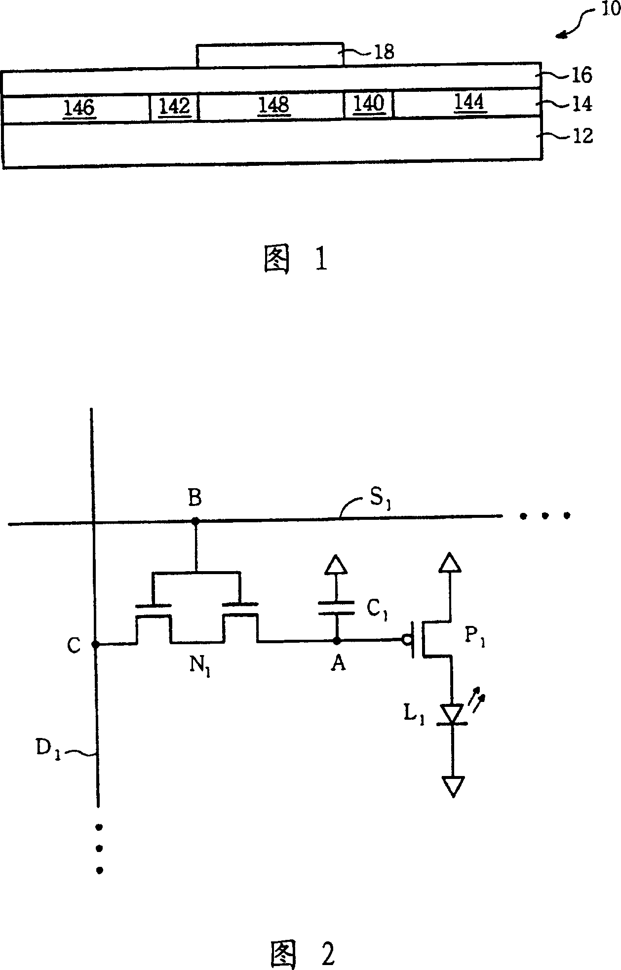
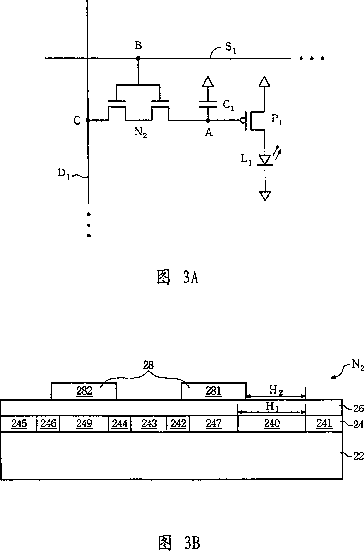
[0034] Please refer to FIG. 3A , which is a schematic diagram of a pixel circuit in a preferred embodiment of the present invention. The pixel circuit is a driving circuit for a current-driven active light-emitting display, and at least includes a dual-gate thin film transistor N2, a driving transistor P1, a capacitor C1, and a light-emitting diode L1. The source of the double-gate thin film transistor N2 is connected to a data line D1, and the gate is connected to a scan line S1. The gate of the driving transistor P1 is connected to the drain of the dual-gate thin film transistor N2. The capacitor C1 is connected to where the source of the dual-gate thin film transistor N2 and the gate of the driving transistor P1 are connected. The anode of the light emitting diode L1 is connected to the drain of the driving transistor P1. The main difference between this embodiment and the prior art is that the used double-gate thin film transistor N2 has an asymmetric lightly doped drain...


PUM


Abstract

The present invention relates to a pixel circuit for driving several unit pixels in the panel of display device. Said circuit at least includes several scanning lines, several data lines, a lightly-doped drain thin film transistor (LDD-TFT) respectively connected with scanning lines and data lines of unit pixels and a drive transistor. Said lightly-doped drain thin film transistor at least has a first lightly-doped drain and a second lightly-doped drain different in length, in which the first lightly-doped drain closed to drive transistor has longest length.

Description

technical field [0001] The invention relates to a thin film transistor structure with asymmetric lightly doped drain electrodes, in particular to a thin film transistor structure in a pixel circuit of a liquid crystal display. Background technique [0002] With the improvement of semiconductor manufacturing process, thin film transistor (Thin Film Transistor, TFT) components are getting smaller and smaller, and the channel length between the source and drain of the thin film transistor is shortened accordingly. When the channel length of the thin film transistor is shortened, in addition to the decrease of the threshold voltage (Vt), leakage current occurs, and the phenomenon of the hot electron effect (Hot Electron Effect) affects the operation of the transistor. In order to solve this problem, a lightly doped drain (LDD) structure is developed in the prior art to reduce the electric field at the drain junction, so as to reduce the influence of the hot electron effect. [...

Claims


Application Information

Patent Timeline
Patent Type & Authority Patents(China)
IPC IPC(8): G09G3/20H01L29/786
Inventor 唐宇骏施立伟
Owner AU OPTRONICS CORP
Why Eureka
Try Eureka