Heterostructure LED device with enhanced hole injection
A technology for LED devices and heterostructures, applied in semiconductor devices, electrical components, circuits, etc., can solve the problems of increased device operating voltage, harsh epitaxial growth conditions, and complex preparation processes, and achieves increased device operating voltage and improved space. Hole concentration and hole drift rate, the effect of mitigating activation energy
- Summary
- Abstract
- Description
- Claims
- Application Information
AI Technical Summary
Problems solved by technology
Method used
Image

Examples
Embodiment 1
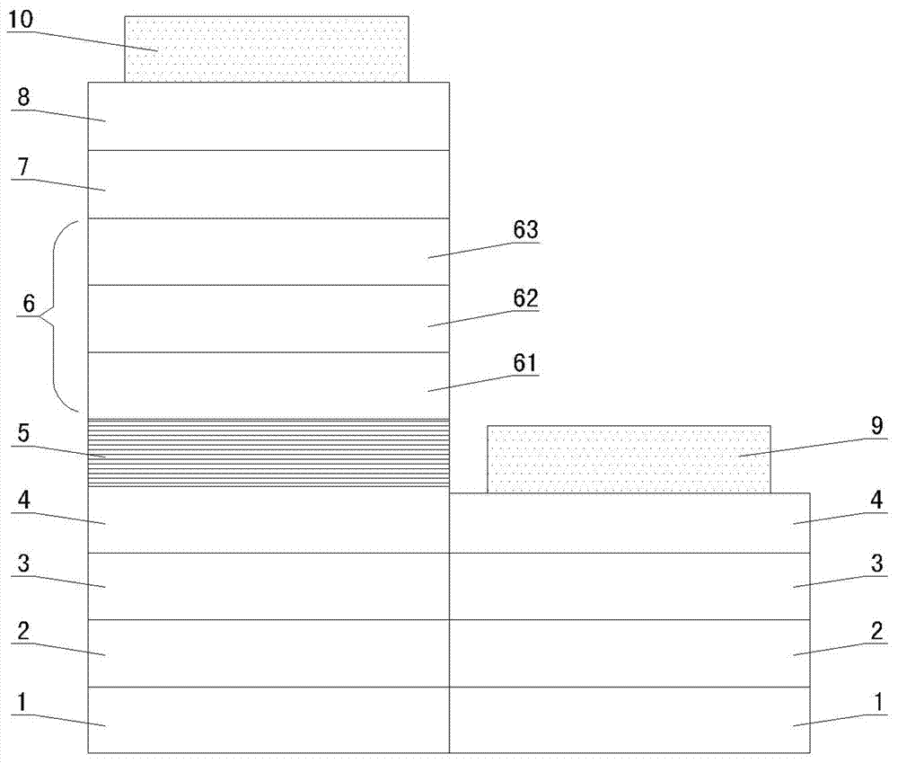
[0018]In this embodiment, the LED device is a blue LED device with a formal structure, and its structure is as follows: figure 1 shown. At this time, the substrate 1 is a patterned sapphire growth substrate, on which a GaN buffer layer, a GaN unintentionally doped layer, an n-type GaN electron Drift layer, 10 cycles of In 0.2 Ga 0.8 N / GaN multi-quantum well light-emitting active region (light-emitting wavelength is about 460nm), p-type electron blocking layer, p-type GaN hole drift layer and p-type GaN contact layer. The conditions and parameters of epitaxial growth are similar to those of traditional high-power blue LEDs. The difference is that the p-type electron blocking layer is made of p-Al with a thickness of 5nm 0.14 Ga 0.86 N layer, p-In with a thickness of 1nm / 1nm / 1nm in sequence 0.08 Ga 0.92 N / p-In 0.04 Ga 0.96 N / p-In 0.14 Ga 0.86 N composite layer and p-Al with a thickness of 5nm 0.07 Ga 0.93 N layer composition. The Mg doping concentration is 3×10 19...
Embodiment 2
[0021] In this embodiment, the LED device is a near-ultraviolet LED device with a formal structure, and its structure is as follows: figure 1 shown. At this time, the substrate 1 is a sapphire / AlN composite growth substrate, on which a GaN buffer layer, a GaN unintentionally doped layer, an n-type Al 0.07 Ga 0.93 N electron drift layer, 10 cycles of In 0.08 Ga 0.92 N / GaN multi-quantum well light-emitting active region (light-emitting wavelength is about 395nm), p-type electron blocking layer, p-type Al 0.07 Ga 0.93 N hole drift layer and p-type In 0.07 Ga 0.93 N-contact layer. The conditions and parameters of epitaxial growth are similar to those of traditional near-ultraviolet LEDs. The difference is that the p-type electron blocking layer is made of p-Al with a thickness of 2nm 0.15 Ga 0.85 N layer, p-In with a thickness of 2nm / 2nm / 2nm 0.05 Ga 0.95 N / p-In 0.03 Ga 0.97 N / p-In 0.08 Ga 0.92 N composite layer and p-Al with a thickness of 5nm 0.14 Ga 0.86 N lay...
Embodiment 3
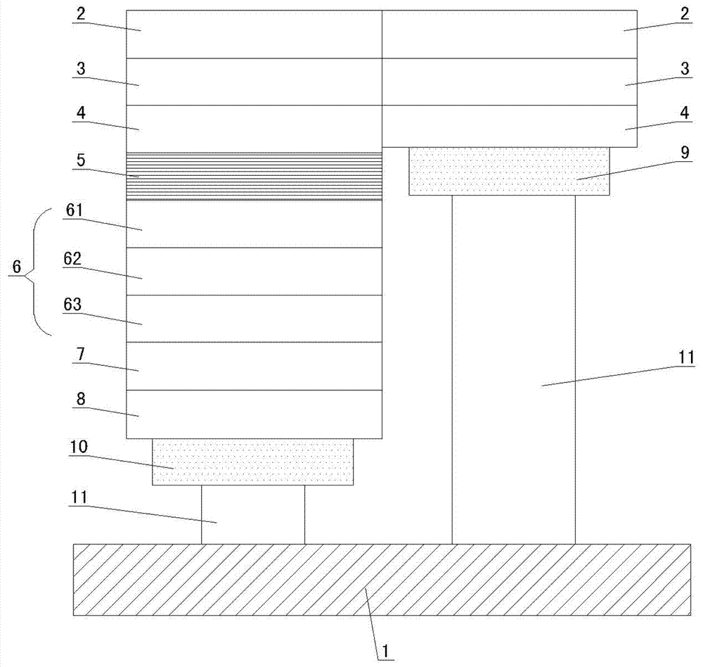
[0024] In this embodiment, the LED device is a near-ultraviolet LED device with a flip-chip structure, and its structure is as follows: figure 2 shown. At this time, the substrate 1 is a thermally conductive base. Its epitaxial structure is an AlN buffer layer, AlN buffer layer, Al 0.3 Ga 0.7 N unintentionally doped layer, n-type Al 0.1 Ga 0.9 N electron drift layer, 10 cycles of In 0.02 Ga 0.98 N / Al 0.1 Ga 0.9 N multi-quantum well light-emitting active region (light-emitting wavelength is about 365nm), p-type electron blocking layer, p-type Al 0.1 Ga 0.9 N hole drift layer and p-type In 0.02 Ga 0.98 N-contact layer. The conditions and parameters of epitaxial growth are similar to those of traditional near-ultraviolet LEDs. The difference is that the p-type electron blocking layer is made of p-Al with a thickness of 3nm 0.2 Ga 0.8 N layer, p-In with a thickness of 3nm / 3nm / 3nm 0.02 Ga 0.98 N / p-In 0.02 Ga 0.98 N / p-In 0.02 Ga 0.98 N composite layer and p-Al ...
PUM
 Abstract
Description
Claims
Application Information