
Method for preparing ultrathin silicon nitride/silicon dioxide laminated gate medium

A technology of silicon dioxide and stacked gates, applied in semiconductor/solid-state device manufacturing, semiconductor devices, electrical components, etc., can solve the problem of high production cost

Inactive Publication Date: 2008-07-02
SEMICON MFG INT (SHANGHAI) CORP +1
View PDF3 Cites 0 Cited by
  • Summary
  • Abstract
  • Description
  • Claims
  • Application Information

AI Technical Summary

Problems solved by technology

These methods require special equipment and are expensive to manufacture

Method used


Image

  • Method for preparing ultrathin silicon nitride/silicon dioxide laminated gate medium
  • Method for preparing ultrathin silicon nitride/silicon dioxide laminated gate medium
  • Method for preparing ultrathin silicon nitride/silicon dioxide laminated gate medium

Examples


Embodiment

[0033] 1. Monolayer growth:

[0034] 1) Ultra-thin SiO 2 Preparation of gate dielectric:

[0035] Note 14 N + , re-oxidation method to reduce the oxidation rate; at the same time reduce the oxidation temperature and reduce the oxidation time to prepare an ultra-thin oxygen pad layer. The oxidation conditions are as follows:

[0036] Note 14 N + : Energy is 20kev, dose: 3E14cm -2 ;

[0037] Oxidation temperature: 690°C;

[0038] Oxidation time: 2s;

[0039] N 2 :O 2 =25:1.

[0040] 2. Preparation of ultra-thin Si by LPCVD method 3 N 4 membrane;

[0041] Using TEMPRESS 280 equipment to prepare ultra-thin Si 3 N 4 Film, the equipment has good process repeatability, and the deposited film has good uniformity. The reaction source gas adopts: SiH 2 Cl 2 and NH 3 , the reaction equation is as follows:

[0042] 3SiH 2 Cl 2 (gas)+4NH 3 (gas) → Si 3 N 4 (solid)+6H 2 (gas)

[0043] In order to prepare ultra-thin Si 3 N 4 film, to improve the controllability...


PUM


Abstract

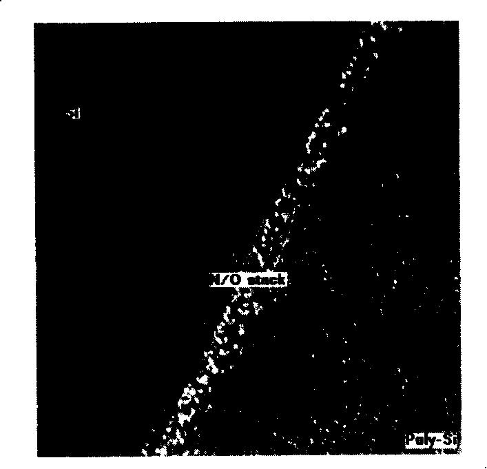
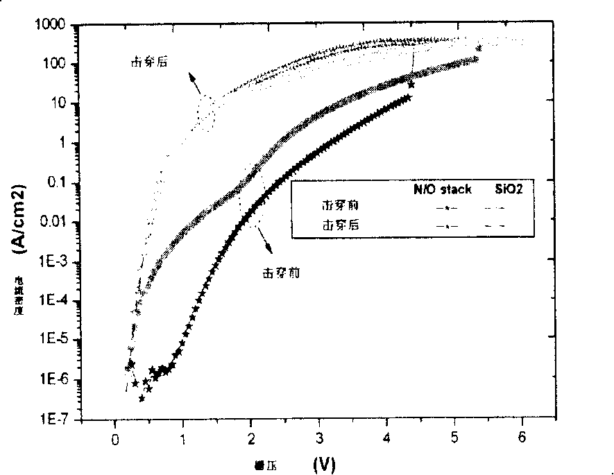
Using conventional low-pressure chemical vapor deposition (LPCVD) method in low cost prepares ultrathin Si3N4 film so as to obtain ultrathin grid medium of Si3N4 / SiO2 stack with equivalent oxidizing layer thickness (EOT) being as 1.9nm in fine performance. Based on the groundwork, the invention makes a scrutiny into characteristics of the said grid medium of Si3N4 / SiO2 (N / O) stack, and applies it to developing CMOS device of high performance N / O stack grid medium with grid length being as 0.13 mum. The invention discloses a convenient feasible method for preparing high performance grid medium needed for deep submicro CMOS device.

Description

technical field [0001] The invention belongs to the field of semiconductor devices, and in particular relates to a method for preparing an ultra-thin silicon nitride / silicon dioxide laminated gate dielectric. Background technique [0002] As the feature size of integrated circuits continues to decrease, SiO, which is the core of traditional CMOS devices, 2 The thickness of the gate dielectric is also reduced accordingly, and the resulting problems are the sharp increase of gate tunneling current and impurities penetrating the gate dielectric into the silicon substrate (mainly boron penetration). These two problems will seriously affect the performance of CMOS devices, and even cause the device to fail. [0003] Si 3 N 4 The material has been widely studied because of its high dielectric constant and good resistance to impurity penetration. It has been reported that the JVD (Jet Vapor Deposition) method has been used to prepare Si with excellent characteristics such as low...

Claims


Application Information

Patent Timeline
Patent Type & Authority Patents(China)
IPC IPC(8): H01L21/336H01L21/28H01L21/314
Inventor 林刚徐秋霞
Owner SEMICON MFG INT (SHANGHAI) CORP
Learn More