Technology for making composite crystal structure

A technology of composite crystal and sheet structure, which is applied in semiconductor/solid-state device manufacturing, electrical components, circuits, etc., and can solve problems such as increasing process complexity.

Inactive Publication Date: 2008-07-02
SINO AMERICAN SILICON PROD
View PDF7 Cites 0 Cited by
  • Summary
  • Abstract
  • Description
  • Claims
  • Application Information

AI Technical Summary

Problems solved by technology

However, using the existing technology to mass-produce the composite wafer structure, edge damage is not guaranteed not to occur
In addition, several prior art techniques add to the complexity of the process

Method used


Image

  • Technology for making composite crystal structure
  • Technology for making composite crystal structure
  • Technology for making composite crystal structure

Examples


Embodiment Construction

[0027] The present invention provides a method for manufacturing a composite wafer structure, in particular, fracture is actively controlled during the composite wafer fabrication process, thereby avoiding edge damage of the composite wafer structure. Several preferred specific embodiments according to the present invention are disclosed as follows.

[0028] Please refer to Figure 2A to Figure 2H as shown, Figure 2A to Figure 2H is a sectional view for describing the manufacturing method according to the first preferred embodiment of the present invention.

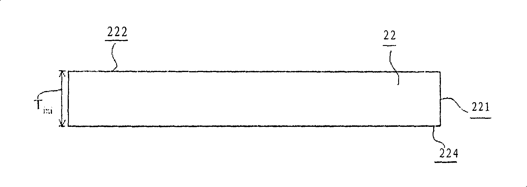
[0029] First, if Figure 2A As shown, a device wafer 22 is prepared. The device wafer 22 has a first circumference (Circumference) 221 , a bonding surface 222 and a bottom surface 224 .

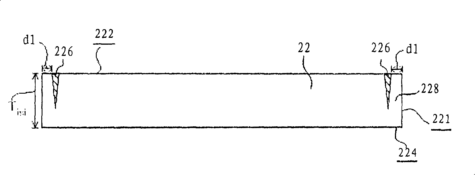
[0030] Next, on the bonding surface 222 of the device wafer 22, a groove (Groove) 226 is formed along the first circumference 221 of the device wafer 22, such as Figure 2B shown. It should be noted that there is a margin (Margin)...


PUM


Abstract

This invention provides one compound crystal structure method, which actively controls the induced breakage during process based on breakage force theory to avoid fringe damage. This invention method can improve compound crystal structure product rate in industry volume.

Description

technical field [0001] The present invention relates to a method for manufacturing a composite wafer structure, and in particular, the present invention relates to a method for manufacturing a composite wafer structure that actively controls fracture during the manufacturing process, thereby avoiding edge damage (Edge Wafer) of the composite wafer structure. damage). Background technique [0002] The composite wafer structure has been widely used as the substrate of semiconductor technology or MEMS technology, for example, silicon-on-insulator (SOI) structure. Hereinafter, a typical SOI structure is taken as an example to illustrate the edge damage that often occurs in the manufacturing process of the composite wafer structure. [0003] Please refer to figure 1 , a cross-sectional view of a typical SOI structure 1 is depicted in figure 1 middle. The SOI structure 1 basically includes a device wafer (Device wafer) 12 and a base wafer (Base wafer) 14 . [0004] like figu...

Claims


Application Information

Patent Timeline
Patent Type & Authority Patents(China)
IPC IPC(8): H01L21/762
Inventor 叶哲良黄菁仪徐文庆何雅兰许松林王荣宗
Owner SINO AMERICAN SILICON PROD
Why Eureka
Try Eureka