Supercharge Your Innovation With Domain-Expert AI Agents!

Solid-state image pickup apparatus, and pixel data read voltage applying method

A camera device and voltage technology, applied in radiation control devices, televisions, electrical components, etc., can solve the problems of large vertical shift register area and reduced size of camera equipment.

Inactive Publication Date: 2008-08-20
FUJITSU MICROELECTRONICS LTD
View PDF5 Cites 0 Cited by
  • Summary
  • Abstract
  • Description
  • Claims
  • Application Information

AI Technical Summary

Problems solved by technology

[0016] However, in these two documents, vertical shift registers are provided on both sides of the two-dimensional pixel array, and the area of ​​the vertical shift registers is large, which cannot solve the problem that the size of the imaging device is difficult to be reduced

Method used


Image

  • Solid-state image pickup apparatus, and pixel data read voltage applying method
  • Solid-state image pickup apparatus, and pixel data read voltage applying method
  • Solid-state image pickup apparatus, and pixel data read voltage applying method

Examples


Embodiment Construction

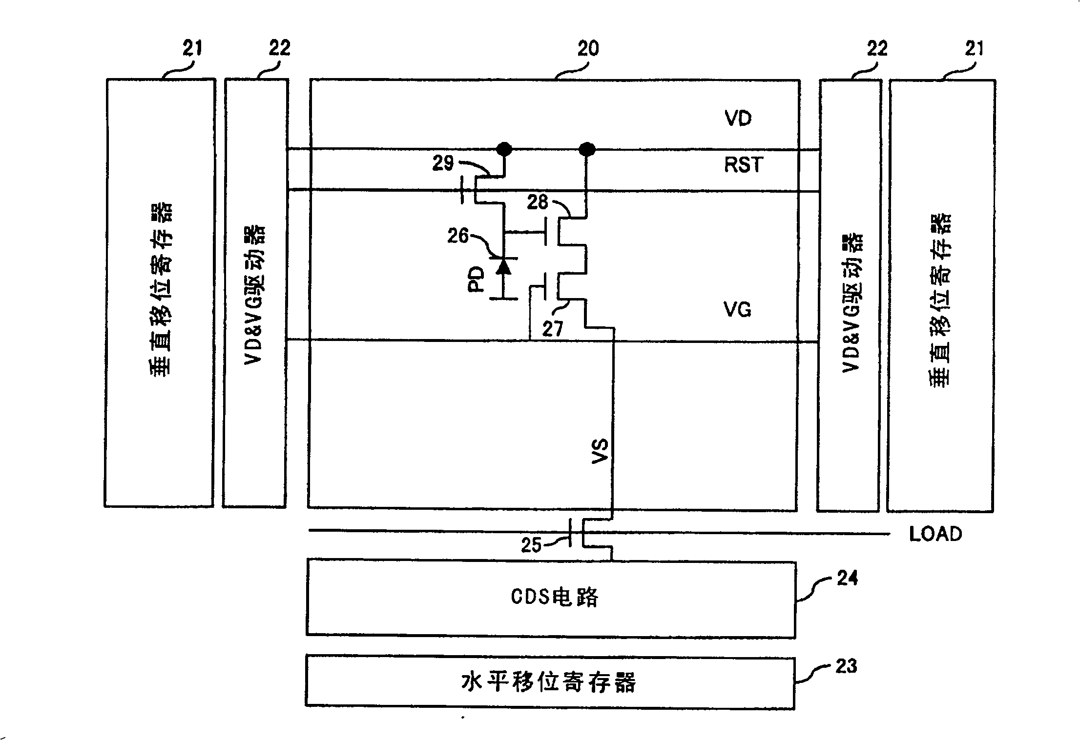
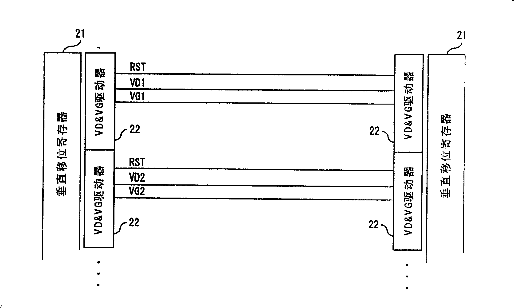
[0031] Figure 4 is a configuration block diagram showing the principle of the solid-state imaging device according to the present invention. Figure 4 A schematic configuration of a solid-state imaging device having pixels in the form of a two-dimensional pixel array is shown, and includes at least a two-dimensional pixel array 1 , a vertical shift register 2 , and a voltage applying device 3 .

[0032] The vertical shift register 2 outputs a selection signal for selecting a horizontal pixel sequence in the two-dimensional pixel array, and provides the selection signal to the pixel array 1 from the left outer side or the right outer side of the pixel array 1 .

[0033] After the vertical shift register 2 outputs the selection signal, the voltage applying device 3 applies the power supply voltage for reading data of the horizontal pixel sequence to the pixel array 1 from the side opposite to the output selection signal.

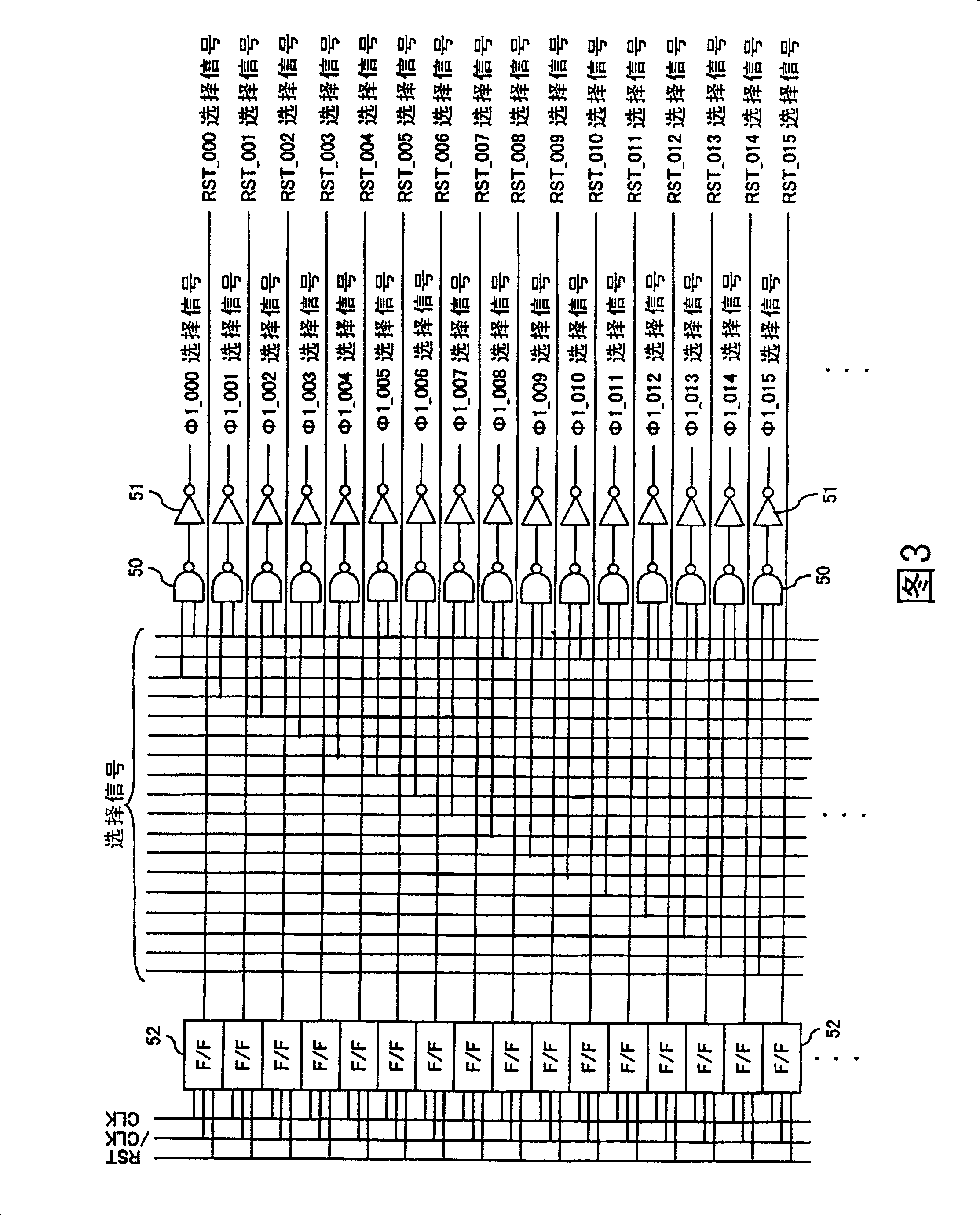
[0034] In the embodiment of the present invention, a v...


PUM


Abstract

A shift register outputs a selection signal for selection of a horizontal sequence of pixels of a two-dimensional pixel array, and includes a vertical shift register for applying a selection signal to the pixel array from either the outer left side or the outer right side of the pixel array, and a voltage applying device for applying a power supply voltage for reading data for a horizontal sequence of pixels from an opposite side of a supply of the selection signal to the pixel array after the selection signal is output.

Description

technical field [0001] The present invention relates to a solid-state imaging device such as a CMOS sensor, and more particularly to a solid-state imaging device having a vertical shift register located on one side of a pixel array for selecting A horizontal pixel sequence in a two-dimensional pixel array, the solid-state imaging device provides pixel data reading voltages from both sides of the pixel array while reducing the layout area. Background technique [0002] Conventionally, a solid-state imaging device having, for example, photoelectric conversion devices arranged in a two-dimensional array in vertical and horizontal directions, and using a plurality of transistors to read charges accumulated in the respective photoelectric conversion devices is generally used. [0003] figure 1 is a block diagram showing the configuration of the above-described conventional solid-state imaging device. exist figure 1 , the device comprises a pixel array 20 surrounded by: a verti...

Claims


Application Information

Patent Timeline
Patent Type & Authority Patents(China)
IPC IPC(8): H01L27/146H04N5/335H04N5/225H04N25/00H04N25/65
CPCH04N5/3742H04N5/3577H04N25/617H04N25/767
Inventor 柳沢诚井上忠夫山本克义
Owner FUJITSU MICROELECTRONICS LTD
Features
  • R&D
  • Intellectual Property
  • Life Sciences
  • Materials
  • Tech Scout
  • Unparalleled Data Quality
  • Higher Quality Content
  • 60% Fewer Hallucinations
Learn More