Stack organic electroluminescent cell and its manufacturing method

A technology for electroluminescent components and manufacturing methods, which is applied in the fields of electrical components, semiconductor/solid-state device manufacturing, electro-solid-state devices, etc. Effect

Inactive Publication Date: 2008-12-17
CHUNGHWA PICTURE TUBES LTD
View PDF5 Cites 0 Cited by
  • Summary
  • Abstract
  • Description
  • Claims
  • Application Information

AI Technical Summary

Problems solved by technology

However, if figure 1 The structure shown only has the luminous effect of monochrome or white light, which cannot meet the requirement of full color

Method used


Image

  • Stack organic electroluminescent cell and its manufacturing method
  • Stack organic electroluminescent cell and its manufacturing method
  • Stack organic electroluminescent cell and its manufacturing method

Examples


no. 1 example

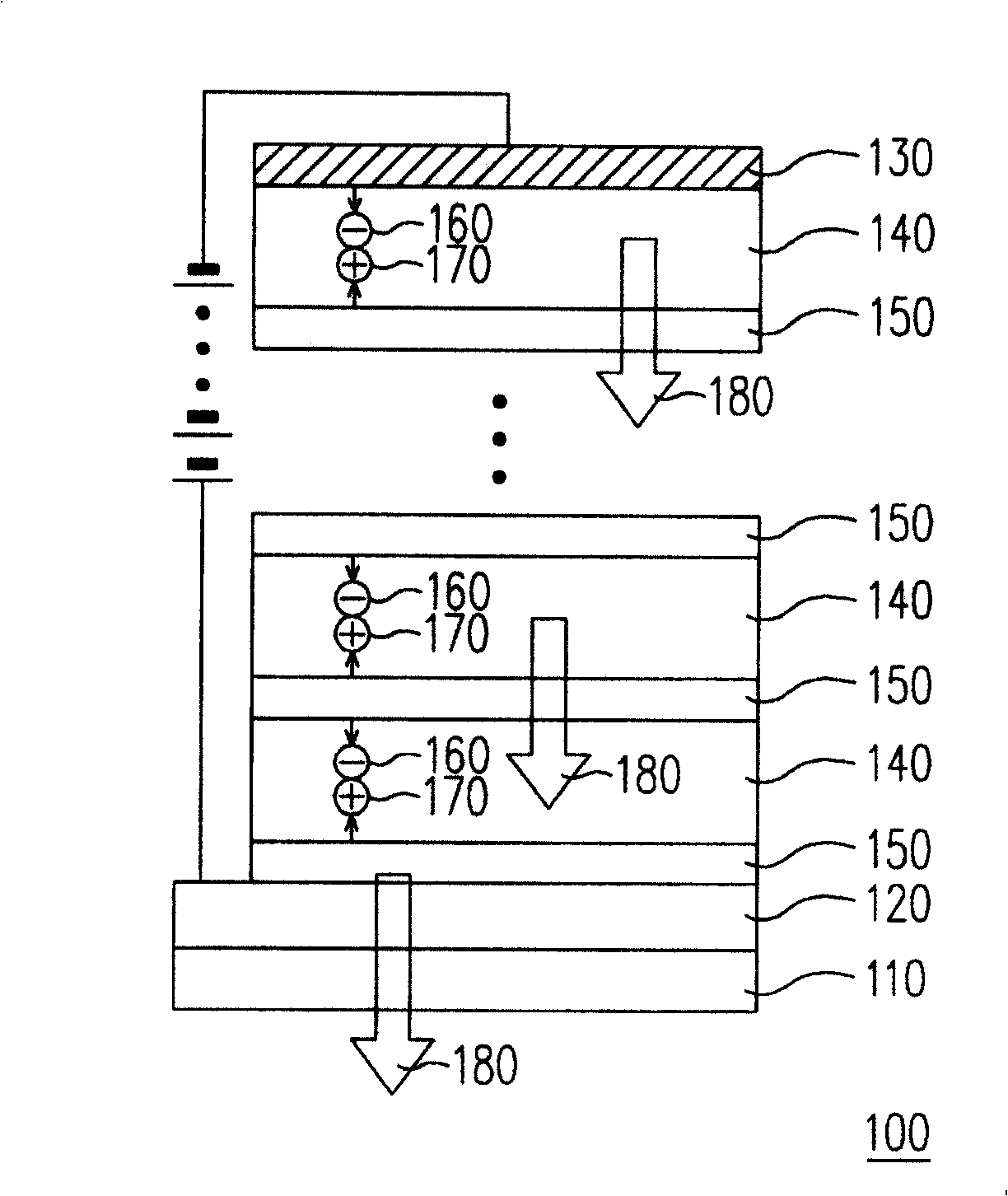
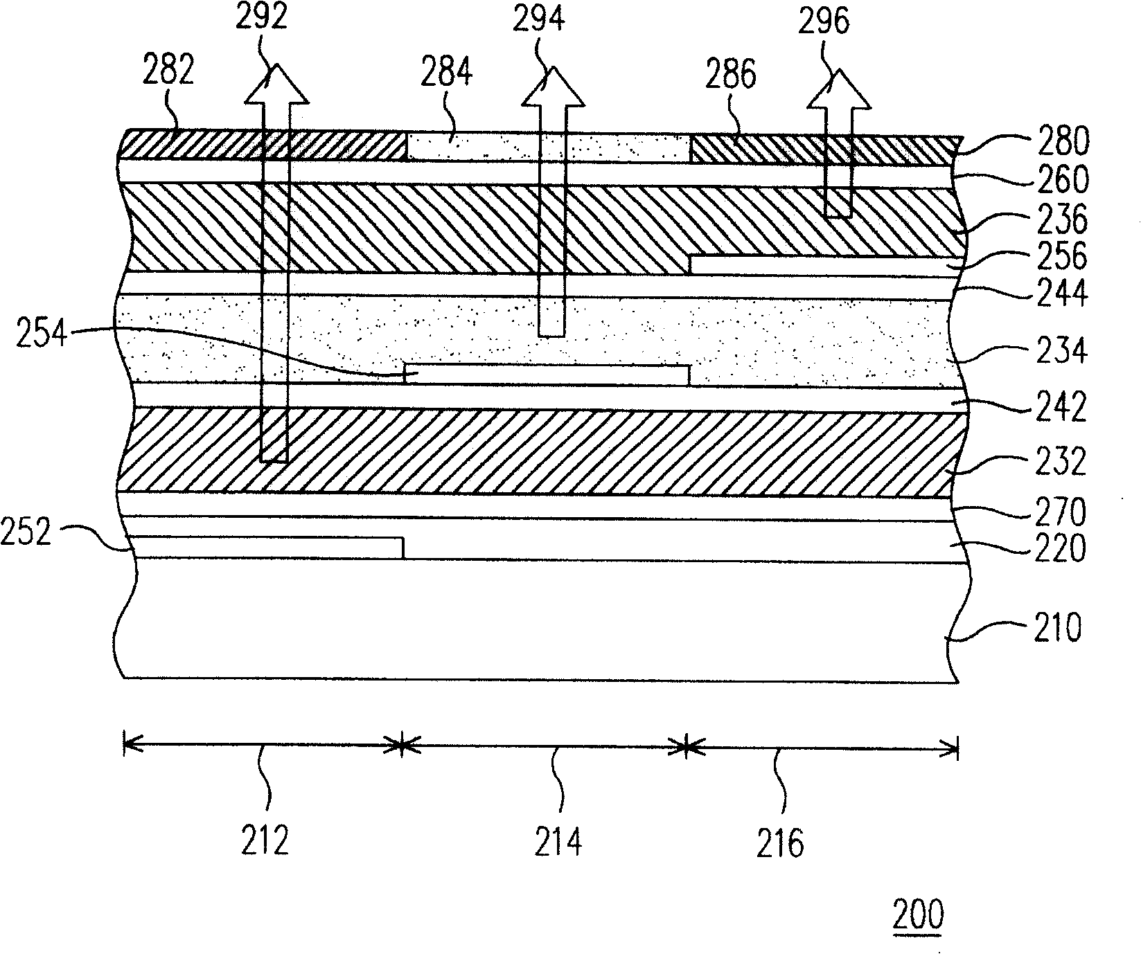
[0064] figure 2 It is a schematic structural view of a stacked organic electroluminescence element in a preferred embodiment of the present invention. Please refer to figure 2 , the stacked organic electroluminescent element 200 includes a substrate 210, an anode layer 220, a plurality of organic light emitting layers 232, 234, 236, a plurality of carrier generation layers 242, 244, a plurality of reflective layers 252, 254, 256 and Cathode layer 260 . Wherein, the substrate 210 has a first light emitting region 212 , a second light emitting region 214 and a third light emitting region 216 . The anode layer 220 is disposed on the substrate 210 . The organic light emitting layer 232 is disposed on the anode layer 220 . The organic light emitting layer 234 is disposed on the organic light emitting layer 232 . The organic light emitting layer 236 is disposed on the organic light emitting layer 234 . The carrier generation layer 242 is disposed between the organic light em...

no. 2 example

[0078] Figure 6A ~ Figure 6E It is a schematic flowchart of the steps of a method for manufacturing a stacked organic electroluminescent device in a preferred embodiment of the present invention. Please refer to as Figure 6A ~ Figure 6E With the steps shown, the process is a continuous process.

[0079] First, if Figure 6A As shown, a substrate 210 having a first light emitting region 212 , a second light emitting region 214 and a third light emitting region 216 is provided. The substrate 210 is, for example, a plastic substrate or a glass substrate.

[0080] Next, if Figure 6B As shown, a reflective layer 252 is formed on the first light emitting region 212 . The reflective layer 252 is disposed in the first light emitting region 212 and on the substrate 210 . The method of forming the reflective layer 252 is, for example, using the patterned mask 310 in conjunction with the evaporation process 320 to form the reflective layer 252 in the first light emitting region ...


PUM


Abstract

The invention relates to a stack organic electroluminescent element, which comprises base plate, anode layer, several organic lighting layers, several carrier generating layers, several reflective layers and cathode layer. Wherein, the base plate has the first lighting area, the second lighting area and the third lighting layer; the anode layer is above the base plate; and above the anode layer, there are first organic lighting layer, first carrier generating layer, second organic lighting layer, second carrier generating layer and third organic lighting layer; the first, second and third reflective layers are inside the stack structure, while they are relative to the first, second and third lighting areas; the cathode layer is above the third organic lighting layer. The invention has better lighting efficiency and better color purity.

Description

technical field [0001] The present invention relates to an organic electroluminescent device and a manufacturing method thereof, and in particular to a stacked organic electro-luminescent device (Stacked Organic Electro-Luminesance Device, Stacked OLED) and a manufacturing method thereof. Background technique [0002] An organic electroluminescent device is a device that utilizes the self-luminous properties of organic functional materials to achieve display effects, and its light-emitting structure is usually composed of a pair of electrodes and an organic functional material layer. When the current passes through the region between the anode and the cathode, electrons and holes are recombined in the organic functional material layer to generate excitons (photons), which can make the organic functional material layer produce different photons according to the characteristics of the material. The light emitting mechanism of the color. [0003] In the manufacture of full-col...

Claims


Application Information

Patent Timeline
Patent Type & Authority Patents(China)
IPC IPC(8): H01L51/50H01L51/56H01L27/32
Inventor 罗世奎汤舜钧吴界煌闾俊中
Owner CHUNGHWA PICTURE TUBES LTD
Why Eureka
Try Eureka