Stacked photovoltaic device
A photoelectric element, laminated technology, applied in the direction of electrical elements, photovoltaic power generation, electric solid state devices, etc., can solve the problems of undisclosed, different film quality and light degradation characteristics, etc.
- Summary
- Abstract
- Description
- Claims
- Application Information
AI Technical Summary
Problems solved by technology
Method used
Image

Examples
Embodiment 1
[0163]
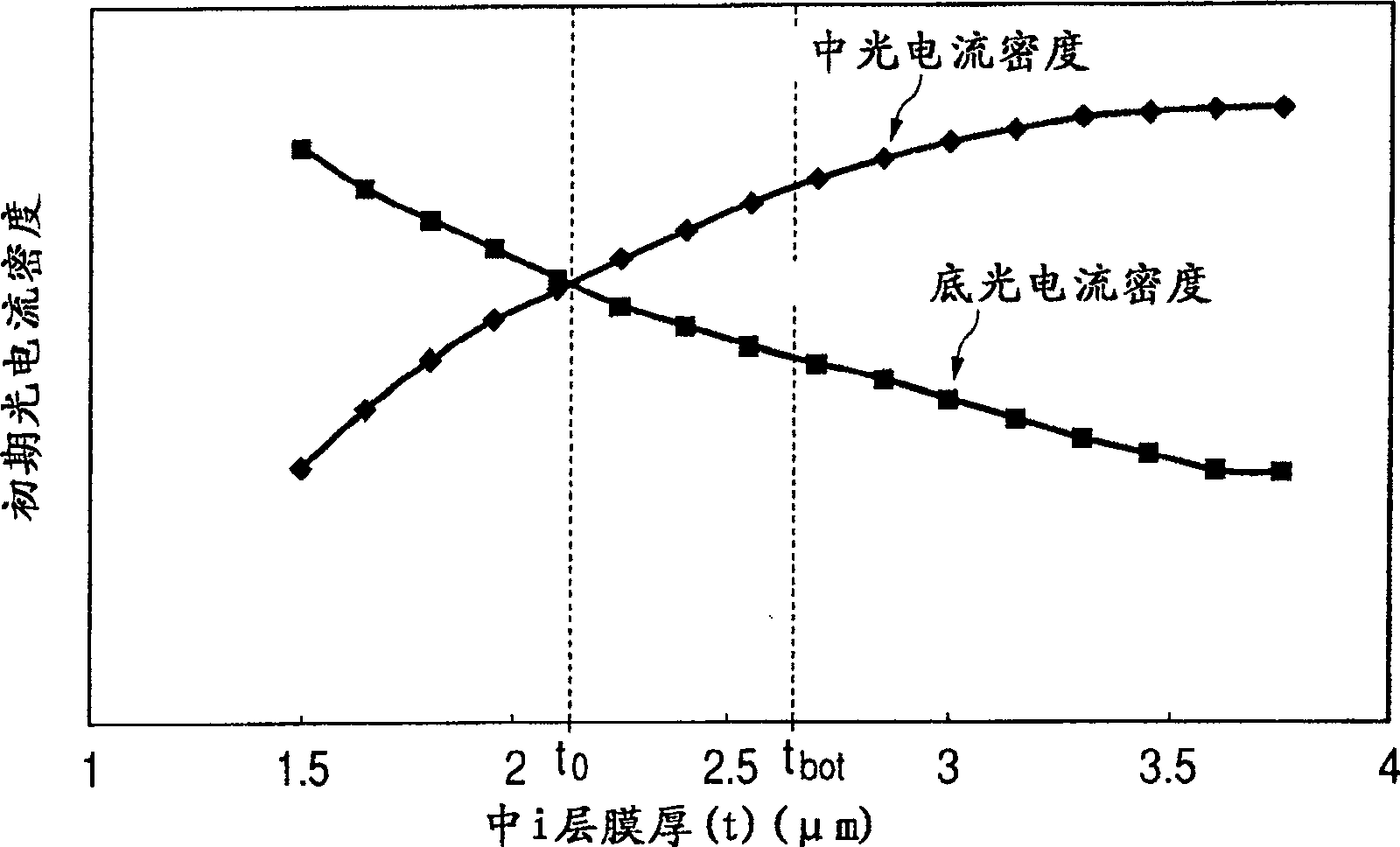
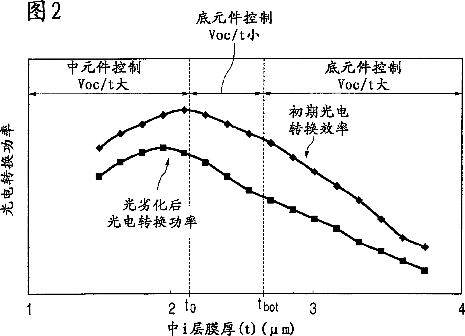
[0164] The multilayer photovoltaic element of this example was deposited by the deposited film forming apparatus shown in FIG. 5 . Table 3 shows common stacking conditions used in Example 1 and Comparative Example 1. Fabrication conditions are selected such that the i-type semiconductor layer of the top element is amorphous silicon, and the i-type semiconductor layers of the middle and bottom elements are microcrystalline silicon. The film thickness of the i-type semiconductor layer of the element in Example 1 is 2.0 μm, and a three-element with the middle element as the control element and the Voc / t of the middle element is larger than the Voc / t of the bottom element is produced. In Comparative Example 1, the film thickness of the element was increased to 2.5 μm, the bottom element was used as the control element, and the Voc / t value was still the largest among the three elements of the middle element.
[0165] table 3
[0166]
[0167] In Table 4, the value o...
Embodiment 2
[0172] (Example 2, Comparative Example 2)
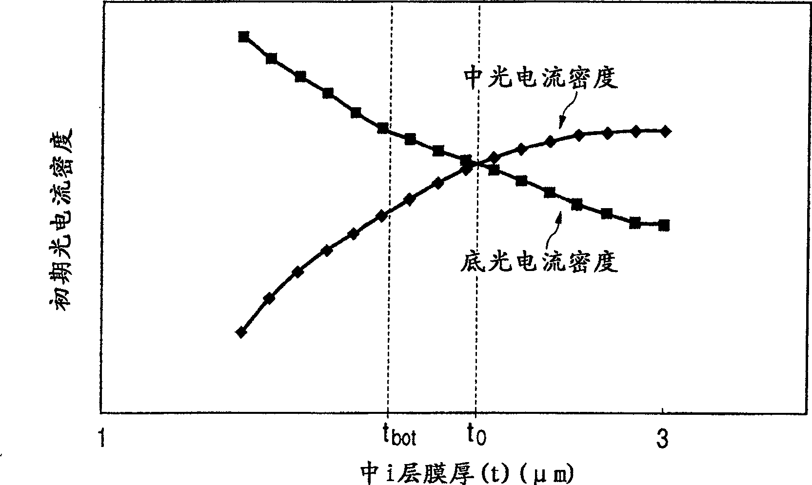
[0173] In this embodiment, by adjusting the film thickness and film-forming conditions of the reflection-enhancing film, compared with the reflection-enhancing film used in Example 1, the texture degree of the surface of the reflection-enhancing film is greatly improved. Thereby, the number of photons absorbed by the bottom element can be increased, and the film thickness of the bottom i layer can be reduced. However, in Example 2, each semiconductor layer was formed under the conditions shown in Table 3, except that the film thickness of the i layer of the bottom element was reduced to 2.0 μm. As in Example 1, the i-type semiconductor layer of the top element is amorphous silicon, and the i-type semiconductor layers of the middle element and the bottom element are microcrystalline silicon. The thickness of the i-type semiconductor layer of the element in Example 2 is 2.5 μm, and a three-element with the top element as the control e...
Embodiment 3、 comparative example 3-1、3-2
[0180] In this embodiment 3, in addition to the formation conditions of the n-type semiconductor layer of the bottom element, the n-type dopant gas, namely pH 3 The flow rate was increased to 20 times that of Example 1, and each semiconductor layer was formed under the same conditions as in Example 1 shown in Table 3. By increasing the pH 3 It was found that the Voc increased, but by reducing the short-circuit photocurrent density of the bottom element, it became the bottom control element, and the same value was obtained as the photoelectric conversion efficiency. This is considered to be due to the influence of the diffusion of P into the i-type semiconductor layer. Actually, SiMS measurement was performed, and the P concentration in the bottom i-type semiconductor layer was higher than that in the bottom i-type semiconductor layer of Example 1 on average by half a digit. In addition, as in Example 1 and Example 2, the P concentration in the middle i layer was negligibly l...
PUM
 Abstract
Description
Claims
Application Information
 - R&D
- Intellectual Property
- Life Sciences
- Materials
- Tech Scout
- Unparalleled Data Quality
- Higher Quality Content
- 60% Fewer Hallucinations
Browse by: Latest US Patents, China's latest patents, Technical Efficacy Thesaurus, Application Domain, Technology Topic, Popular Technical Reports.
© 2025 PatSnap. All rights reserved.Legal|Privacy policy|Modern Slavery Act Transparency Statement|Sitemap|About US| Contact US: help@patsnap.com