Semiconductor chip local electronic radiation method and device

An electron irradiation and semiconductor technology, which is applied in the manufacture of semiconductor/solid-state devices, circuits, electrical components, etc., can solve the problem of not involving or involving the control of local electronic irradiation of the chip, etc., to achieve simple processing, safe and reliable use, low cost effect

CN100533669CActive Publication Date: 2009-08-26ZHUZHOU CRRC TIMES SEMICON CO LTD
4 Cites 0 Cited by

Patent Information

Authority / Receiving Office
CN · China
Patent Type
Patents(China)
Current Assignee / Owner
Publication Date
2009-08-26

Smart Images

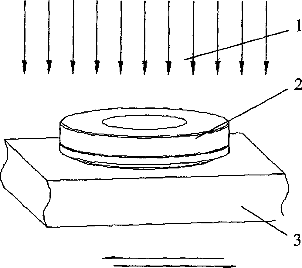
  • Figure 1
    Figure 1
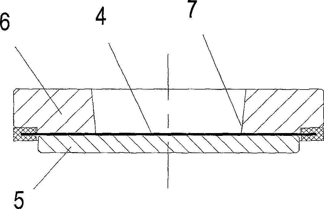
  • Figure 2
    Figure 2
Patent Text Reader

Abstract

A method and device for local electron irradiation of a semiconductor chip. The chip is placed on an "electron linear accelerator" irradiation bed in the electron irradiation area of ​​the chip, and a partitioned electron irradiation device is used to partially block the electron irradiation method to realize semiconductor irradiation. Different regions on the chip are locally irradiated with electrons. The method for partially shielding electron radiation is to use the principle that metal stoppers can isolate electron rays, and set metal stoppers of different thicknesses that can isolate electron rays to block electron rays in parts that do not need or require different electron irradiation doses. The irradiated electron beam realizes the independent electron irradiation of different regions on the semiconductor chip. In particular, the stopper made of metal lead blocks the electron rays on the part of the chip that does not need to be irradiated, so as to realize partial electron irradiation on different regions on the semiconductor chip.
Need to check novelty before this filing date? Find Prior Art

Description

technical field

[0001] The invention relates to a processing method and device for a semiconductor device, in particular to a method and device for local electron irradiation of a semiconductor chip of a power electronic thyristor device. The technology of the invention is mainly used for chips of high-power thyristor devices In the electron irradiation process, such as the positioning electron irradiation of the diode part in the reverse conduction GCT device, it can also be used for the partial electron irradiation treatment of the chip of other semiconductor components. Background technique

[0002] During the chip processing of many semiconductor devices, electron irradiation treatment must be carried out on its surface. Since most of the traditional high-power thyristor and diode processing adopt uniform electron irradiation technology, this electron irradiation method is harmful to the same semiconductor chip. Different regions cannot carry out independent electronic r...

Examples

Embodiment Construction

[0016] The present invention will be further described below in conjunction with the accompanying drawings and embodiments.

[0017] pass figure 1 It can be seen that the present invention relates to a method for electron irradiation of semiconductor element chips. The chip is placed on the irradiation bed of the irradiation device, and a partitioned electron irradiation device is used to partially shield the electron rays during electron irradiation to realize the irradiation of electrons. Different areas on the semiconductor chip are locally irradiated with electrons. The method for partially shielding electron radiation is to use the principle that metal stoppers can isolate electron rays, and set metal stoppers of different thicknesses that can isolate electron rays to block electron rays in parts that do not need or require different electron irradiation doses. The irradiated electron beam realizes partial electron irradiation of different regions on the semiconductor ch...