Semiconductor chip local electronic radiation method and device

An electron irradiation and semiconductor technology, which is applied in the manufacture of semiconductor/solid-state devices, circuits, electrical components, etc., can solve the problem of not involving the local electronic irradiation control of the chip, not involved, etc., to achieve safe and reliable use, simple processing, low cost effect

Active Publication Date: 2008-03-19
ZHUZHOU CRRC TIMES SEMICON CO LTD
View PDF2 Cites 6 Cited by
  • Summary
  • Abstract
  • Description
  • Claims
  • Application Information

AI Technical Summary

Problems solved by technology

Mainly through three different ways of irradiation and post-irradiation annealing process to optimize the overall parameters of the device, but does not involve local electron irradiation control in different regions; Chinese patent application (patent application number is 200510011701.6; The title is "high-power fast soft recovery diode and its production process") also discloses a high-power semiconductor device manufacturing process, which also refers to chip electron irradiation and other processes, but the invention te

Method used


Image

  • Semiconductor chip local electronic radiation method and device

Examples


Embodiment Construction

[0016] The present invention will be further described below in conjunction with the accompanying drawings and embodiments.

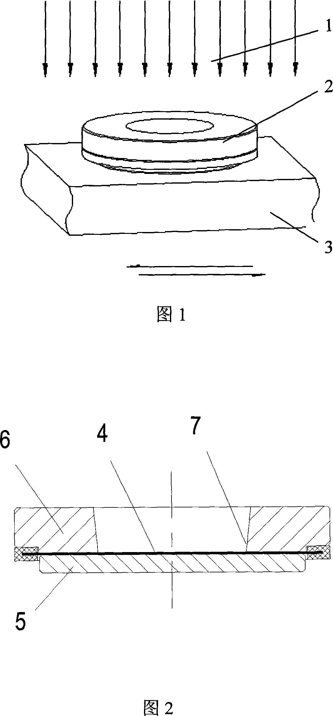
[0017] It can be seen from Fig. 1 that the present invention relates to a method for electron irradiation of semiconductor element chips. The chip is placed on the irradiation bed of the irradiation device, and a method of partially shielding electron rays during electron irradiation is adopted through a partitioned electron irradiation device. , to achieve local electron irradiation on different regions on the semiconductor chip. The method for partially shielding electron radiation is to use the principle that metal stoppers can isolate electron rays, and set metal stoppers of different thicknesses that can isolate electron rays to block electron rays in parts that do not need or require different electron irradiation doses. The irradiated electron beam realizes partial electron irradiation of different regions on the semiconductor chip. In particula...


PUM


Abstract

A local electron irradiation method and a device for a semiconductor chip are provided, which comprises placing a chip on an irradiation bed of an electron linear accelerator in the electron irradiation zone of the chip, and performing the local electron irradiation to the different zones on the semiconductor chip by using the partial mask electron irradiation method. The partial mask electron irradiation method, based on the principle that metal barrier can isolate electron rays, arranges electron ray-isolating metal barriers with different thicknesses in the parts apart from electron irradiation or in need of electron irradiation with different doses, thereby realizing the independence electron irradiation to individual zones on the semiconductor chip. In particular, the lead metal barrier is used to block the electron ray for the chip parts apart from electron irradiation, thereby realizing the local electron irradiation of individual zones on the semiconductor chip.

Description

technical field [0001] The invention relates to a processing method and device for a semiconductor device, in particular to a method and device for local electron irradiation of a semiconductor chip of a power electronic thyristor device. The technology of the invention is mainly used for chips of high-power thyristor devices In the electron irradiation process, such as the positioning electron irradiation of the diode part in the reverse conduction GCT device, it can also be used for the partial electron irradiation treatment of the chip of other semiconductor components. Background technique [0002] During the chip processing of many semiconductor devices, electron irradiation treatment must be carried out on its surface. Since most of the traditional high-power thyristor and diode processing adopt uniform electron irradiation technology, this electron irradiation method is harmful to the same semiconductor chip. Different regions cannot carry out independent electronic r...

Claims


Application Information

Patent Timeline
IPC IPC(8): H01L21/268
Inventor 张明李继鲁蒋谊陈芳林
Owner ZHUZHOU CRRC TIMES SEMICON CO LTD
Why Eureka
Try Eureka