Laser beam machine

A laser instrument and laser beam technology, applied in the field of laser instruments, can solve the problems of difficult to divide workpiece processing failure areas, and the degraded layer cannot be uniformly exposed.

Active Publication Date: 2009-10-14
DISCO CORP
View PDF9 Cites 0 Cited by
  • Summary
  • Abstract
  • Description
  • Claims
  • Application Information

AI Technical Summary

Problems solved by technology

Although the focus of the pulsed laser beam is set at a predetermined distance from the top surface of the workpiece so that the degenerated layer is exposed to the top surface of the workpiece, when the top surface of the workpiece is uneven, the degraded layer cannot be uniformly exposed to the top surface of the workpiece
In this case, it will be difficult to divide the workpiece along the degraded layer of processing failure zone

Method used


Image

  • Laser beam machine
  • Laser beam machine
  • Laser beam machine

Examples


Embodiment Construction

[0022] The laser apparatus according to the preferred embodiment of the present invention will be described in detail below with reference to the accompanying drawings.

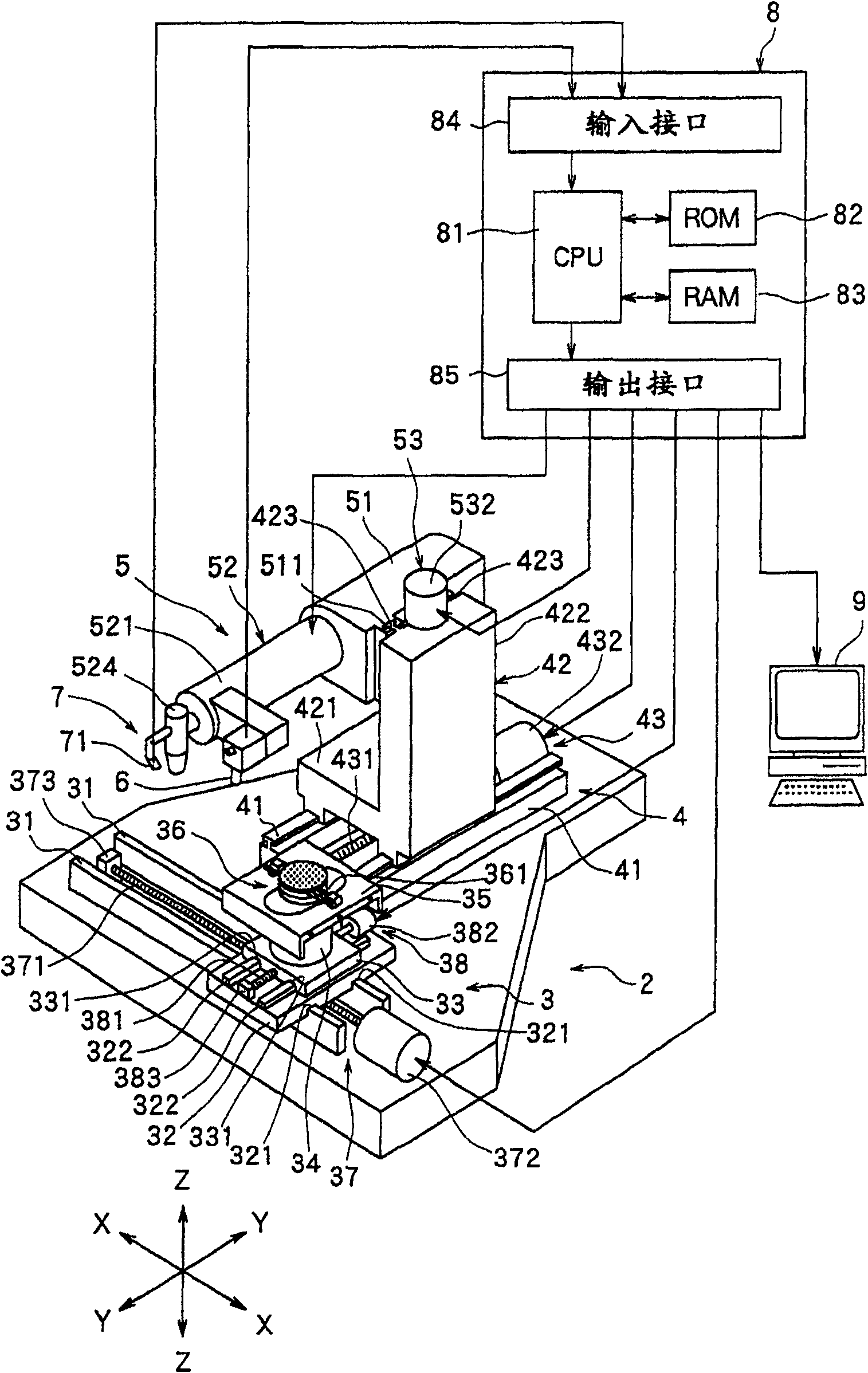
[0023] figure 1 It is a perspective view of a laser instrument manufactured according to the present invention. figure 1 The laser instrument shown in includes: a fixed base 2; a chuck table mechanism 3 for clamping a workpiece, which is mounted on the fixed base 2 in a movable manner along the processing and feeding direction indicated by arrow X; and the laser beam application unit supports The mechanism 4 is mounted on the fixed base 2 in a movable manner along the indexing feed direction indicated by the arrow Y, the direction indicated by the arrow Y is perpendicular to the direction indicated by the arrow X; and the laser beam application unit 5, which It is mounted on the laser beam application unit support mechanism 4 in a movable manner in the direction indicated by arrow Z.

[0024] The above-mention...


PUM

PropertyMeasurementUnit
thicknessaaaaaaaaaa
energyaaaaaaaaaa

Abstract

A kind of laser instrument, described laser instrument comprises the chuck table of clamping wafer and the laser beam application device that applies laser beam to the wafer that clamps on the chuck table to form degraded layer, wherein, described laser instrument further Comprising: a photodetection device for detecting reflected light from a portion of the wafer to be processed, wherein a laser beam emitted from a laser beam application device is applied to the wafer; and a control device for detecting The output of the device judges that the degraded layer has no exposed areas on the top surface of the wafer.

Description

Technical field [0001] The invention relates to a laser instrument for performing predetermined processing on a workpiece with a laser beam. Background technique [0002] In the production process of semiconductor devices, semiconductor wafers are divided into multiple regions by dividing lines called "tracks" which are arranged in a lattice pattern on the front surface of a substantially disc-shaped semiconductor wafer, and A circuit (element) such as IC or LSI is formed on each divided area. The semiconductor wafer is cut along the track of the divided areas to divide it into areas on which circuits are formed, thereby manufacturing individual semiconductor chips. An optical device wafer including a gallium nitride compound semiconductor laminated on the front surface of a sapphire substrate is also cut along a track to form a single optical device, such as a light emitting diode or a laser diode widely used in electrical equipment. [0003] Cutting is usually performed by a cu...

Claims


Application Information

Patent Timeline
Patent Type & Authority Patents(China)
IPC IPC(8): G01N21/27G01N21/88B23K26/03B23K26/00B23K101/40H01L21/301
CPCB23K26/034B23K26/032B23K26/03B23K2201/40B23K2101/40
Inventor 永井祐介小林贤史森重幸雄中村胜村田正博
Owner DISCO CORP
Why Eureka
Try Eureka