Structure embedded with semiconductor chip and its manufacturing method

A semiconductor and chip technology, applied in semiconductor/solid-state device manufacturing, semiconductor devices, semiconductor/solid-state device components, etc., can solve the problems of unable to shorten the molding time, waste of space for substrate panels, low product yield, etc., to achieve improvement The effect of process yield and mass production, reducing board warpage and improving utilization

Active Publication Date: 2009-11-18
PHOENIX PRECISION TECH CORP
View PDF4 Cites 21 Cited by
  • Summary
  • Abstract
  • Description
  • Claims
  • Application Information

AI Technical Summary

Problems solved by technology

However, in the above-mentioned existing manufacturing process, when the semiconductor chip layout is performed on the substrate panel, it is necessary to reserve some areas on the substrate panel for subsequent singulation operations using the forming machine. Since the forming machine is generally relatively large, the The area reserved on the substrate panel is also correspondingly large, thus wasting the circuit layout space available for the substrate, or reducing the typesetting rate of the substrate panel and increasing the cost
[0008] Moreover, in the above-mentioned existing manufacturing process, after the semiconductor chip is directly placed into the substrate panel, the circuit process is performed on a single side surface of the substrate panel, resulting in an unbalanced stress on the opposite surface of the formed packaging structure, which makes the substrate panel easy to process during the manufacturing process. Warpage occurs, resulting in low product yield and difficult production
[0009] Furthermore, in the existing manufacturing process, the molding machine is used to directly cut the packaging substrate panel, so that the molding time cannot be shortened
On the other hand, the circuit is generally made of metal copper. During the singulation operation, the metal copper with high ductility is subjected to the pressure of the forming machine to cause the copper surface to extend, which may easily cause the packaging structure after singulation to overlap. scratches, which in turn damages the packaging structure and reduces production yield
[0010] Therefore, how to provide a structure for embedding semiconductor chips and its manufacturing method, so as to avoid the waste of substrate panel space, low substrate layout rate, substrate warping, package structure damage, low yield rate and increased cost in the prior art Defects such as increased molding time and increased molding time have become problems that the industry needs to overcome urgently.

Method used


Image

  • Structure embedded with semiconductor chip and its manufacturing method
  • Structure embedded with semiconductor chip and its manufacturing method
  • Structure embedded with semiconductor chip and its manufacturing method

Examples


Embodiment Construction

[0050] Embodiments of the present invention are described below through specific examples, and those skilled in the art can easily understand other advantages and effects of the present invention from the contents disclosed in this specification. The present invention can also be implemented or applied through other different specific embodiments, and various modifications and changes can be made to the details in this specification based on different viewpoints and applications without departing from the spirit of the present invention.

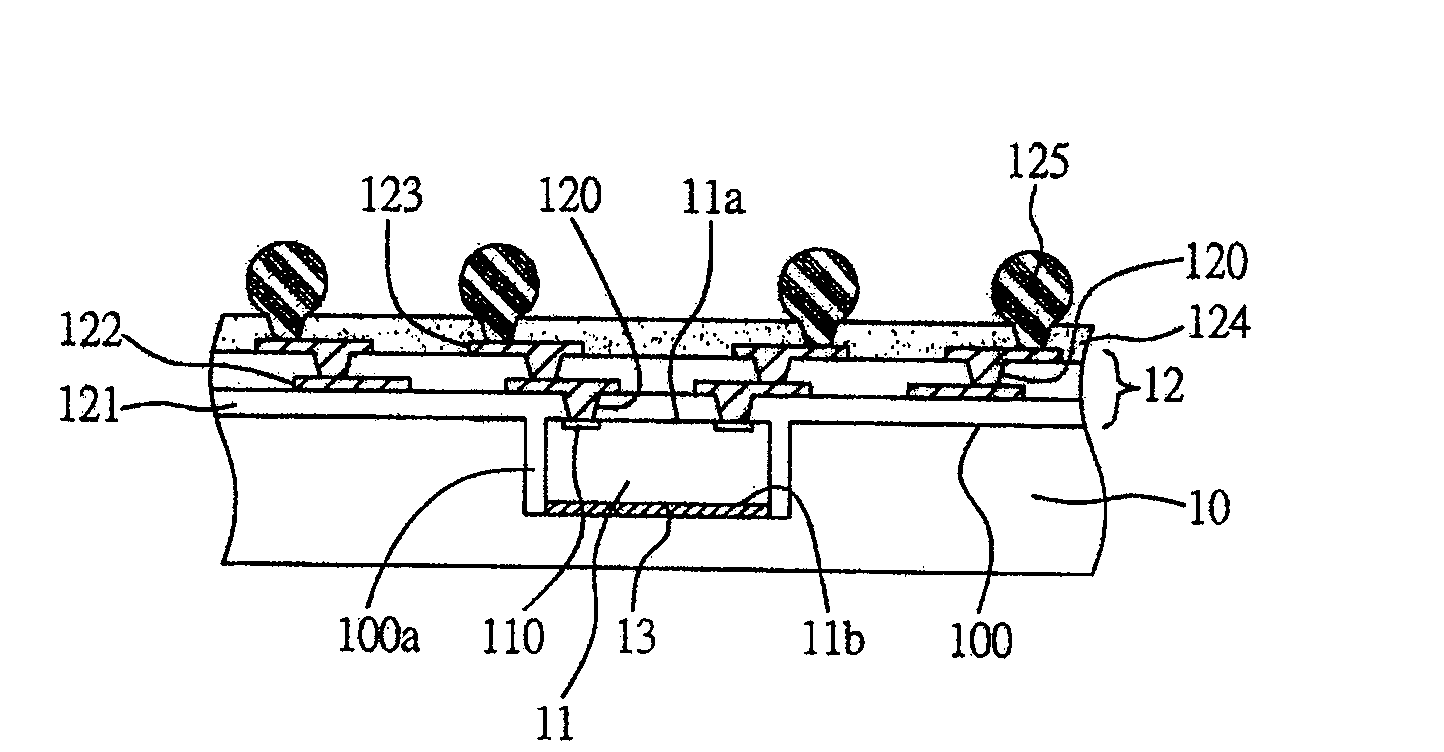
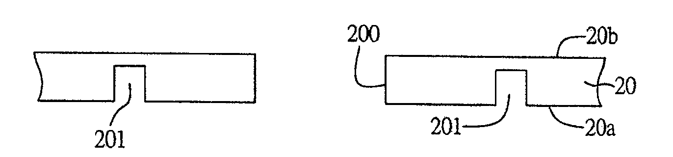
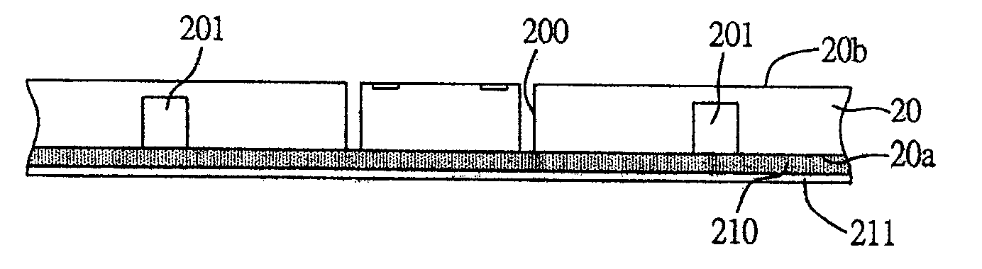
[0051] see Figure 2A to Figure 2I , is a schematic cross-sectional view showing the structure of the embedded semiconductor chip of the present invention. It should be noted that the above-mentioned drawings are all simplified schematic diagrams, and only schematically illustrate the manufacturing process of the circuit board of the present invention. However, the accompanying drawings only show elements related to the present invention, a...


PUM


Abstract

The present invention discloses a structure of a embedded semiconductor chip and its manufacturing method, the method mostly provides a loading plate opposing first and second surface, forming multi- through opening in the loading plate, and forming first plow groove surrounding the opening and without through the loading plate at the first surface of the loading plate, and placing the semiconductor chip in the opening severalty, and pressing the first surface of the loading plate and the semiconductor chip on the first dielectric layer for stuffing the first dielectric layer into the first plow groove and the gapping place between the semiconductor chip and the loading plate, forming the second plow groove at the second surface corresponding to the first plow groove position, and the second plow groove is communicated with the first plow groove to forming the plow groove through the loading plate, thereby the subsequent cutting operation can be executed by the through plow groove, furthermore the loading plate space is used efficiently and the typesetting rate is improved, and the molding time is reduced.

Description

technical field [0001] The invention relates to a structure and a manufacturing method of an embedded semiconductor chip, in particular to a structure and a manufacturing method of an embedded semiconductor chip integrated with a semiconductor chip and a circuit structure at the same time. Background technique [0002] With the vigorous development of the electronic industry, electronic products are also developing in the direction of lightness, thinness, shortness, smallness, high integration and multi-function. In order to meet the high integration (Integration) and miniaturization (Miniaturization) packaging requirements of semiconductor packages, the packaging shape of semiconductor chips has gradually evolved from single-chip ball grid array (BGA) packaging or flip-chip (FlipChip, FC) packaging to 3D packaging and modular packaging forms have resulted in different packaging structures such as SiP (System in Package), SIP (System Integrated Package), SiB (System in Board...

Claims


Application Information

Patent Timeline
Patent Type & Authority Patents(China)
IPC IPC(8): H01L21/50H01L21/60H01L23/12H01L23/498
CPCH01L2224/04105H01L2224/73267H01L24/19H01L2224/0401H01L2924/15153H01L2224/32225H01L2224/12105H01L2224/19H01L2924/00012
Inventor 曾昭崇许诗滨
Owner PHOENIX PRECISION TECH CORP
Why Eureka
Try Eureka