CMOS image sensor and fabricating method thereof

A technology of image sensor and manufacturing method, which is applied in semiconductor/solid-state device manufacturing, electric solid-state devices, semiconductor devices, etc., and can solve problems such as inability to provide voltage and device performance degradation

Inactive Publication Date: 2010-02-24
DONGBU HITEK CO LTD
View PDF4 Cites 0 Cited by
  • Summary
  • Abstract
  • Description
  • Claims
  • Application Information

AI Technical Summary

Problems solved by technology

If electrons are lost from the floating diffusion (FD) due to leakage, the device cannot provide the correct voltage
Therefore, device performance is degraded

Method used


Image

  • CMOS image sensor and fabricating method thereof
  • CMOS image sensor and fabricating method thereof
  • CMOS image sensor and fabricating method thereof

Examples


Embodiment Construction

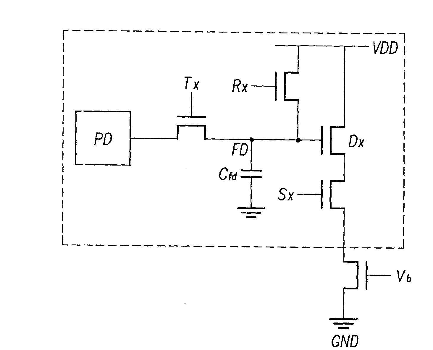
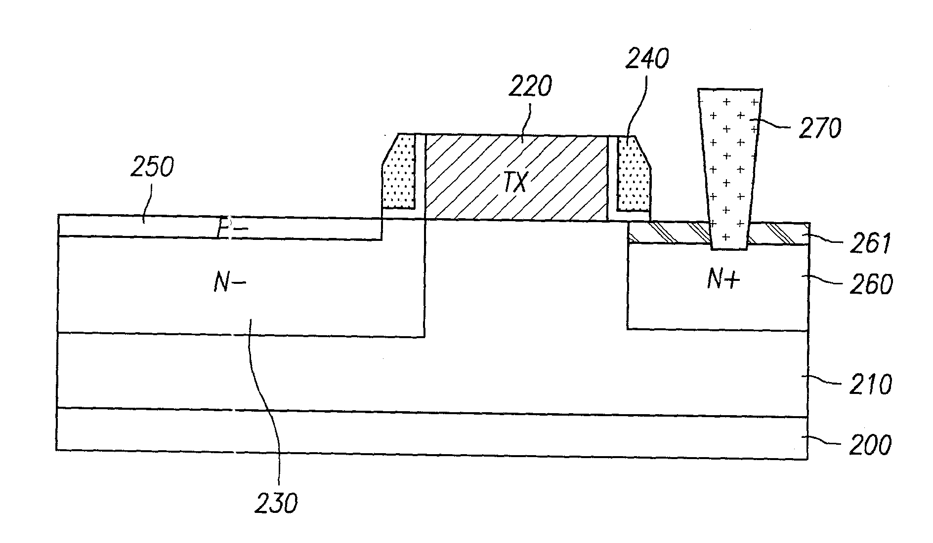
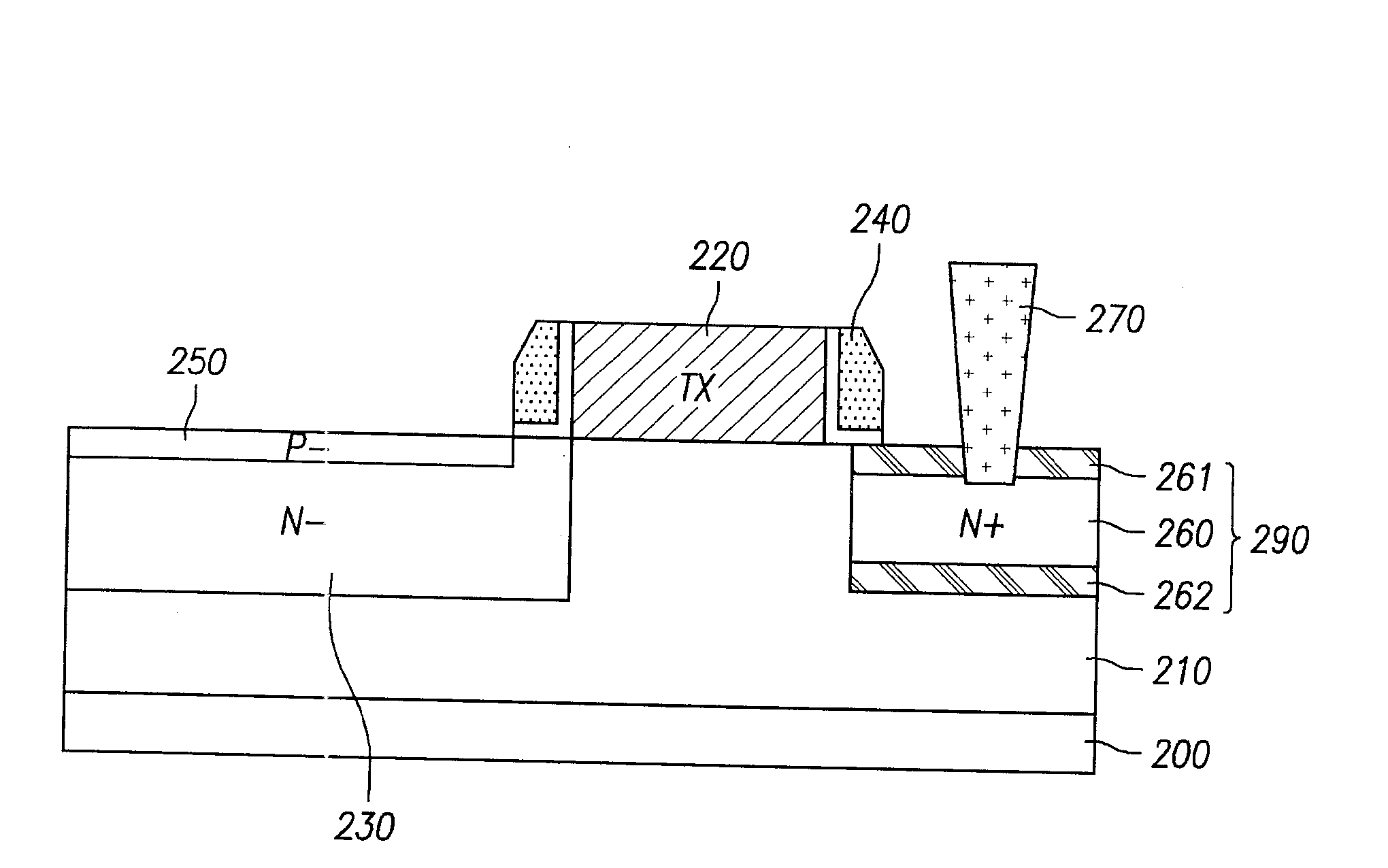
[0012] example Figure 2a with 2b Schematically shows the transfer transistor T x the gate, photodiode region, and floating diffusion region. In particular, a reset transistor (R x ), drive transistor (D x ) and select transistor (S x ).

[0013] Refer to example Figure 2a , the lightly doped p- epitaxial layer 210 is grown on the heavily doped p+ substrate 200 . A device isolation layer for inter-unit-pixel isolation may be formed at a designated portion of the p-epitaxial layer 210 by local oxidation of silicon (LOCOS) or shallow trench isolation (STI). Subsequently, the transfer transistor (T x ) gate (hereinafter abbreviated as gate 220 ) is formed on the p- epitaxial layer 210 .

[0014] The deep n-diffusion layer 230 is formed by lightly implanting n-type impurities (n-) with high energy into the portion of the p- epitaxial layer 210 immediately adjacent to the gate 220 . When forming the n-diffusion layer 230, an n-very lightly doped drain (VLDD) region can b...


PUM


Abstract

A CMOS image sensor and method of manufacture reduces the problem of electron loss in a floating diffusion area. A method of fabricating a CMOS image sensor includes forming a gate electrode over a first conductive type semiconductor substrate. A second conductive type first diffusion layer is formed within the semiconductor substrate to be aligned with an edge of one side of the gate electrode. Aspacer may be attached to both sidewalls of the gate electrode. A first conductive type second diffusion layer may be formed within the first diffusion layer to leave a distance amounting to a widthof the spacer in-between. A second conductive type third diffusion layer may be formed within the semiconductor substrate to be aligned with an edge of the other side of the gate electrode. A first conductive type fourth diffusion layer may be formed over the third diffusion layer, and a first conductive type fifth diffusion layer may be formed under the third diffusion layer.

Description

technical field [0001] The present invention relates to a CMOS image sensor, in particular to a CMOS image sensor and a manufacturing method thereof. While the present invention is suitable for a wide range of applications, it is particularly well suited for solving the problem of electron leakage from floating diffusions. Background technique [0002] According to the design rules of CMOS technology, CMOS image sensors use MOS transistors as photosensitive pixels. Around the periphery of the photosensitive area, the sensor integrates control circuits and signal processing circuits to sequentially detect outputs using MOS transistors. Thereby the CMOS image sensor is more conveniently driven in various scanning modes. Due to the compatibility of CMOS technology, the signal processing circuit can be integrated on a single chip in the CMOS image sensor, so the final product can be made smaller and cheaper. In addition, since the power consumption of CMOS image sensors is mu...

Claims


Application Information

Patent Timeline
Patent Type & Authority Patents(China)
IPC IPC(8): H01L21/822H01L21/335H01L27/146H01L29/06H01L29/772
CPCH01L27/14609H01L27/14643H01L27/14689H01L27/146
Inventor 任劲赫
Owner DONGBU HITEK CO LTD
Why Eureka
Try Eureka