Transimpedance amplifier with negative impedance compensation function

A transimpedance amplifier, negative impedance technology, applied in the field of amplifiers

Active Publication Date: 2007-07-18
IND TECH RES INST
View PDF0 Cites 7 Cited by
  • Summary
  • Abstract
  • Description
  • Claims
  • Application Information

AI Technical Summary

Problems solved by technology

Therefore, it is challenging to overcome the above-ment

Method used


Image

  • Transimpedance amplifier with negative impedance compensation function
  • Transimpedance amplifier with negative impedance compensation function
  • Transimpedance amplifier with negative impedance compensation function

Examples


Embodiment Construction

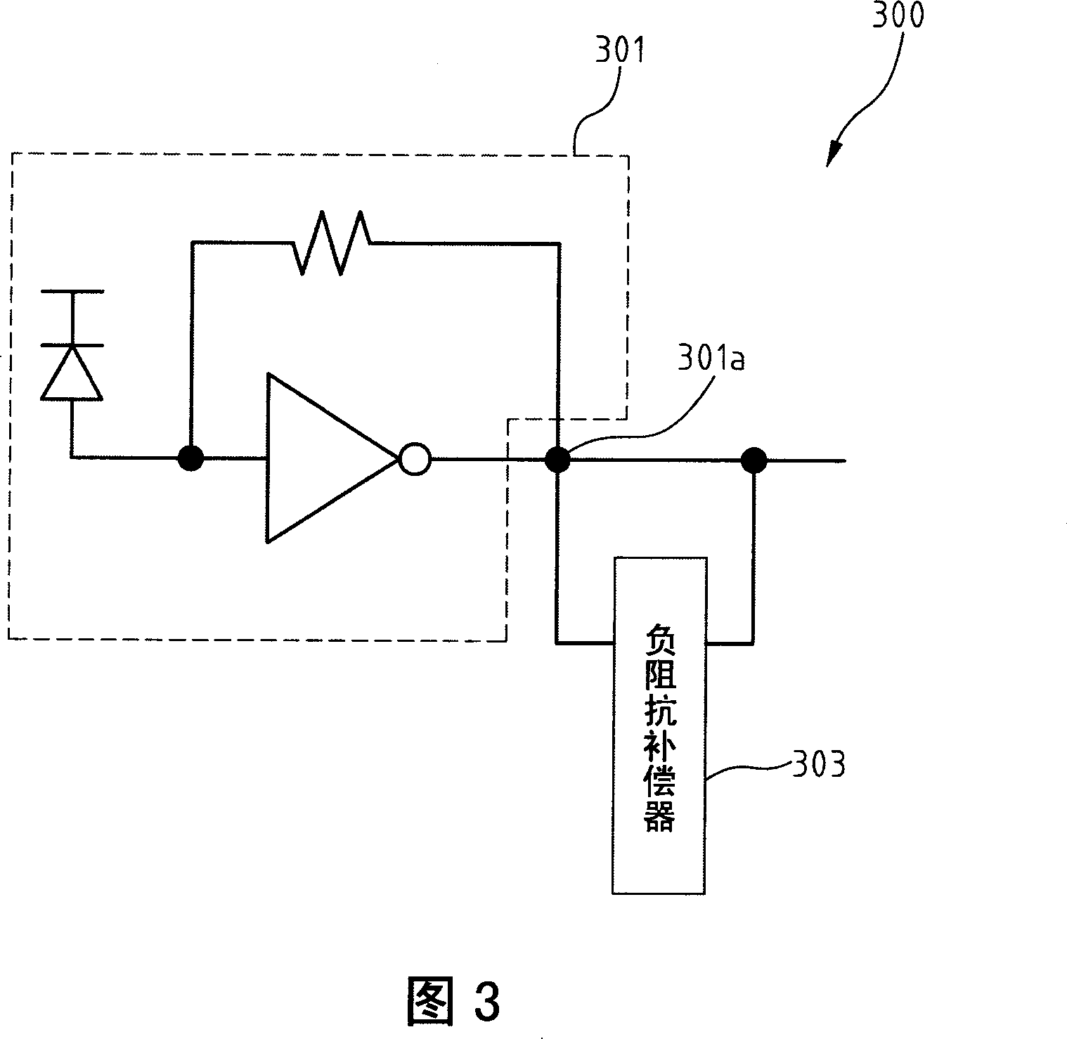
[0048] FIG. 3 is a block diagram illustrating the architecture of the first embodiment of the present invention. Referring to FIG. 3 , the transimpedance amplifier 300 mainly includes a single-stage transimpedance amplifier element 301 and a negative impedance compensator (negativeimpedance compensator) 303 . The single-stage transimpedance amplifier element 301 has an output terminal 301a to generate an equivalent ground impedance. The negative impedance compensator 303 is connected to the output end 301a of the single-stage transimpedance amplifier element 301, which changes the equivalent ground impedance generated by the output end 301a from low to high, and compensates the parasitic capacitance effect generated by the output end 301a .

[0049] The negative impedance compensator 303 can be realized by various circuit architectures, mainly including a negative resistance element composed of a positive feedback circuit and a compensation circuit for the parasitic capacitan...


PUM


Abstract

This invention relates to an impedance-transfer amplifier with a negative impedance compensation function including elements of single-stage impedance-transfer amplifier and a negative impedance compensator connected to the output end of the amplifier element, which is realized in many ways including a negative resistance element composed of positive and negative circuits and a compensation circuit against the parasitic capacitance effect generated by its output end, and the compensator increases the equivalent earth impedance of the output of the single-stage impedance-transfer amplifier and compensates the parasitic capacitance effect.

Description

technical field [0001] The present invention relates to an amplifier in an optical communication system, in particular to a transimpedance amplifier (TIA) with a negative impedance compensation function. Background technique [0002] In an optical communication system, the gain and sensitivity of an optical receiver are very important characteristics, and both must be improved at the same time to optimize transmission performance. As shown in FIG. 1 , the traditional single-stage transimpedance amplifier architecture 100 has a simple structure and high stability, and mainly includes a photo diode 101 and a basic operational amplifier 102 . However, since the overall gain and bandwidth characteristics are closely related to the output impedance of the amplifier, the architecture of this single-stage transimpedance amplifier cannot obtain a high feedback resistance R due to its insufficient voltage gain. F and high sensitivity. [0003] Generally, the architecture of a multi...

Claims


Application Information

Patent Timeline
IPC IPC(8): H03F1/56H03F1/02H03F3/08H04B10/06
Inventor 李岱威蔡嘉明
Owner IND TECH RES INST
Why Eureka
Try Eureka